- 您现在的位置:买卖IC网 > PDF目录3808 > PIC18LF4685-I/PT (Microchip Technology)IC PIC MCU FLASH 48KX16 44TQFP PDF资料下载
参数资料
| 型号: | PIC18LF4685-I/PT |
| 厂商: | Microchip Technology |
| 文件页数: | 39/183页 |
| 文件大小: | 0K |
| 描述: | IC PIC MCU FLASH 48KX16 44TQFP |
| 产品培训模块: | Asynchronous Stimulus 8-bit PIC® Microcontroller Portfolio |
| 标准包装: | 160 |
| 系列: | PIC® 18F |
| 核心处理器: | PIC |
| 芯体尺寸: | 8-位 |
| 速度: | 40MHz |
| 连通性: | CAN,I²C,SPI,UART/USART |
| 外围设备: | 欠压检测/复位,HLVD,POR,PWM,WDT |
| 输入/输出数: | 36 |
| 程序存储器容量: | 96KB(48K x 16) |
| 程序存储器类型: | 闪存 |
| EEPROM 大小: | 1K x 8 |
| RAM 容量: | 3.25K x 8 |
| 电压 - 电源 (Vcc/Vdd): | 2 V ~ 5.5 V |
| 数据转换器: | A/D 11x10b |
| 振荡器型: | 内部 |
| 工作温度: | -40°C ~ 85°C |
| 封装/外壳: | 44-TQFP |
| 包装: | 托盘 |
| 产品目录页面: | 646 (CN2011-ZH PDF) |
第1页第2页第3页第4页第5页第6页第7页第8页第9页第10页第11页第12页第13页第14页第15页第16页第17页第18页第19页第20页第21页第22页第23页第24页第25页第26页第27页第28页第29页第30页第31页第32页第33页第34页第35页第36页第37页第38页当前第39页第40页第41页第42页第43页第44页第45页第46页第47页第48页第49页第50页第51页第52页第53页第54页第55页第56页第57页第58页第59页第60页第61页第62页第63页第64页第65页第66页第67页第68页第69页第70页第71页第72页第73页第74页第75页第76页第77页第78页第79页第80页第81页第82页第83页第84页第85页第86页第87页第88页第89页第90页第91页第92页第93页第94页第95页第96页第97页第98页第99页第100页第101页第102页第103页第104页第105页第106页第107页第108页第109页第110页第111页第112页第113页第114页第115页第116页第117页第118页第119页第120页第121页第122页第123页第124页第125页第126页第127页第128页第129页第130页第131页第132页第133页第134页第135页第136页第137页第138页第139页第140页第141页第142页第143页第144页第145页第146页第147页第148页第149页第150页第151页第152页第153页第154页第155页第156页第157页第158页第159页第160页第161页第162页第163页第164页第165页第166页第167页第168页第169页第170页第171页第172页第173页第174页第175页第176页第177页第178页第179页第180页第181页第182页第183页
2011 Microchip Technology Inc.
DS39931D-page 133
PIC18F46J50 FAMILY
10.1.3
INTERFACING TO A 5V SYSTEM
Though the VDDMAX of the PIC18F46J50 family is 3.6V,
these devices are still capable of interfacing with 5V
systems, even if the VIH of the target system is above
3.6V. This is accomplished by adding a pull-up resistor
to the port pin (Figure 10-2), clearing the LAT bit for that
pin and manipulating the corresponding TRIS bit
(Figure 10-1) to either allow the line to be pulled high,
or to drive the pin low. Only port pins that are tolerant of
voltages up to 5.5V can be used for this type of
interface (refer to Section 10.1.2 “Input Pins and
).
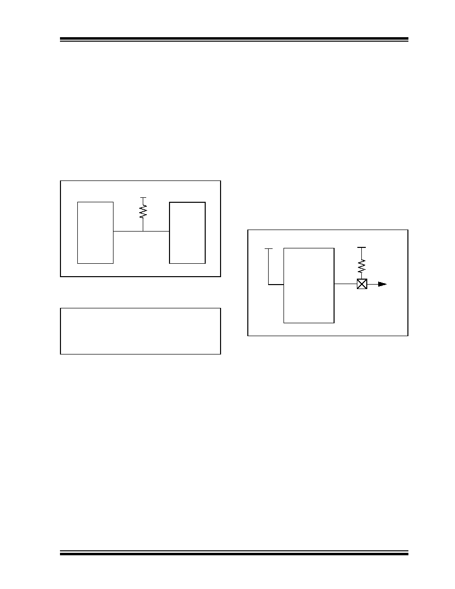
FIGURE 10-2:
+5V SYSTEM HARDWARE
INTERFACE
EXAMPLE 10-1:
COMMUNICATING WITH
THE +5V SYSTEM
10.1.4
OPEN-DRAIN OUTPUTS
The output pins for several peripherals are also
equipped with a configurable open-drain output option.
This allows the peripherals to communicate with
external digital logic, operating at a higher voltage
level, without the use of level translators.
The open-drain option is implemented on port pins
specifically associated with the data and clock outputs
of the EUSARTs, the MSSP modules (in SPI mode) and
the ECCP modules. It is selectively enabled by setting
the open-drain control bit for the corresponding module
in the ODCON registers (Register 10-1, Register 10-2
and Register 10-3). Their configuration is discussed in
more detail with the individual port where these
peripherals are multiplexed. Output functions that are
routed through the PPS module may also use the
open-drain option. The open-drain functionality will
follow the I/O pin assignment in the PPS module.
When the open-drain option is required, the output pin
must also be tied through an external pull-up resistor,
provided by the user, to a higher voltage level, up to
5.5V (Figure 10-3). When a digital logic high signal is
output, it is pulled up to the higher voltage level.
FIGURE 10-3:
USING THE OPEN-DRAIN
OUTPUT (USART SHOWN
AS EXAMPLE)
10.1.5
TTL INPUT BUFFER OPTION
Many of the digital I/O ports use Schmitt Trigger (ST)
input buffers. While this form of buffering works well
with many types of input, some applications may
require TTL level signals to interface with external logic
devices. This is particularly true for the Parallel Master
Port (PMP), which is likely to be interfaced to TTL level
logic or memory devices.
The inputs for the PMP can be optionally configured for
TTL buffers with the PMPTTL bit in the PADCFG1 reg-
ister (Register 10-4). Setting this bit configures all data
and control input pins for the PMP to use TTL buffers.
By default, these PMP inputs use the port’s ST buffers.
RD7
+5V Device
+5V
PIC18F46J50
BCF
LATD, 7
; set up LAT register so
; changing TRIS bit will
; drive line low
BCF
TRISD, 7
; send a 0 to the 5V system
BSF
TRISD, 7
; send a 1 to the 5V system
TXX
+5V
(at logic ‘1’)
3.3V
VDD
5V
PIC18F46J50
相关PDF资料 |
PDF描述 |
|---|---|
| PIC32MX775F512L-80I/BG | IC MCU 32BIT 512KB FLASH 121XBGA |
| PIC32MX795F512H-80I/MR | IC MCU 32BIT 512KB FLASH 64QFN |
| PIC18F6585-I/PT | IC PIC MCU FLASH 24KX16 64TQFP |
| C8051F206 | IC 8051 MCU 8K FLASH 48TQFP |
| PIC16C64A-20/L | IC MCU OTP 2KX14 PWM 44PLCC |
相关代理商/技术参数 |
参数描述 |
|---|---|
| PIC18LF4685T-I/ML | 功能描述:8位微控制器 -MCU 96KB FL 3KB RAM RoHS:否 制造商:Silicon Labs 核心:8051 处理器系列:C8051F39x 数据总线宽度:8 bit 最大时钟频率:50 MHz 程序存储器大小:16 KB 数据 RAM 大小:1 KB 片上 ADC:Yes 工作电源电压:1.8 V to 3.6 V 工作温度范围:- 40 C to + 105 C 封装 / 箱体:QFN-20 安装风格:SMD/SMT |
| PIC18LF46J11-I/ML | 功能描述:8位微控制器 -MCU 64KB Flash 4KBRAM 12MIPS nanoWatt RoHS:否 制造商:Silicon Labs 核心:8051 处理器系列:C8051F39x 数据总线宽度:8 bit 最大时钟频率:50 MHz 程序存储器大小:16 KB 数据 RAM 大小:1 KB 片上 ADC:Yes 工作电源电压:1.8 V to 3.6 V 工作温度范围:- 40 C to + 105 C 封装 / 箱体:QFN-20 安装风格:SMD/SMT |
| PIC18LF46J11-I/PT | 功能描述:8位微控制器 -MCU 64KB Flash 4KBRAM 12MIPS nanoWatt RoHS:否 制造商:Silicon Labs 核心:8051 处理器系列:C8051F39x 数据总线宽度:8 bit 最大时钟频率:50 MHz 程序存储器大小:16 KB 数据 RAM 大小:1 KB 片上 ADC:Yes 工作电源电压:1.8 V to 3.6 V 工作温度范围:- 40 C to + 105 C 封装 / 箱体:QFN-20 安装风格:SMD/SMT |
| PIC18LF46J11T-I/ML | 功能描述:8位微控制器 -MCU 64KB Flash 4KBRAM 12MIPS nanoWatt RoHS:否 制造商:Silicon Labs 核心:8051 处理器系列:C8051F39x 数据总线宽度:8 bit 最大时钟频率:50 MHz 程序存储器大小:16 KB 数据 RAM 大小:1 KB 片上 ADC:Yes 工作电源电压:1.8 V to 3.6 V 工作温度范围:- 40 C to + 105 C 封装 / 箱体:QFN-20 安装风格:SMD/SMT |
| PIC18LF46J11T-I/PT | 功能描述:8位微控制器 -MCU 64KB Flash 4KBRAM 12MIPS nanoWatt RoHS:否 制造商:Silicon Labs 核心:8051 处理器系列:C8051F39x 数据总线宽度:8 bit 最大时钟频率:50 MHz 程序存储器大小:16 KB 数据 RAM 大小:1 KB 片上 ADC:Yes 工作电源电压:1.8 V to 3.6 V 工作温度范围:- 40 C to + 105 C 封装 / 箱体:QFN-20 安装风格:SMD/SMT |
发布紧急采购,3分钟左右您将得到回复。