- 您现在的位置:买卖IC网 > PDF目录3877 > PIC18LF6520T-I/PTG (Microchip Technology)IC MCU FLASH 16KX16 64TQFP PDF资料下载
参数资料
| 型号: | PIC18LF6520T-I/PTG |
| 厂商: | Microchip Technology |
| 文件页数: | 107/165页 |
| 文件大小: | 0K |
| 描述: | IC MCU FLASH 16KX16 64TQFP |
| 标准包装: | 1,200 |
| 系列: | PIC® 18F |
| 核心处理器: | PIC |
| 芯体尺寸: | 8-位 |
| 速度: | 40MHz |
| 连通性: | I²C,SPI,UART/USART |
| 外围设备: | 欠压检测/复位,LVD,POR,PWM,WDT |
| 输入/输出数: | 52 |
| 程序存储器容量: | 32KB(16K x 16) |
| 程序存储器类型: | 闪存 |
| EEPROM 大小: | 1K x 8 |
| RAM 容量: | 2K x 8 |
| 电压 - 电源 (Vcc/Vdd): | 2 V ~ 5.5 V |
| 数据转换器: | A/D 12x10b |
| 振荡器型: | 内部 |
| 工作温度: | -40°C ~ 85°C |
| 封装/外壳: | 64-TQFP |
| 包装: | 带卷 (TR) |
| 其它名称: | PIC18LF6520T-IPTG |
第1页第2页第3页第4页第5页第6页第7页第8页第9页第10页第11页第12页第13页第14页第15页第16页第17页第18页第19页第20页第21页第22页第23页第24页第25页第26页第27页第28页第29页第30页第31页第32页第33页第34页第35页第36页第37页第38页第39页第40页第41页第42页第43页第44页第45页第46页第47页第48页第49页第50页第51页第52页第53页第54页第55页第56页第57页第58页第59页第60页第61页第62页第63页第64页第65页第66页第67页第68页第69页第70页第71页第72页第73页第74页第75页第76页第77页第78页第79页第80页第81页第82页第83页第84页第85页第86页第87页第88页第89页第90页第91页第92页第93页第94页第95页第96页第97页第98页第99页第100页第101页第102页第103页第104页第105页第106页当前第107页第108页第109页第110页第111页第112页第113页第114页第115页第116页第117页第118页第119页第120页第121页第122页第123页第124页第125页第126页第127页第128页第129页第130页第131页第132页第133页第134页第135页第136页第137页第138页第139页第140页第141页第142页第143页第144页第145页第146页第147页第148页第149页第150页第151页第152页第153页第154页第155页第156页第157页第158页第159页第160页第161页第162页第163页第164页第165页
PIC18F6520/8520/6620/8620/6720/8720
DS39609B-page 44
2004 Microchip Technology Inc.
4.3
Fast Register Stack
A “fast interrupt return” option is available for interrupts.
A Fast Register Stack is provided for the Status, WREG
and BSR registers and is only one in depth. The stack
is not readable or writable and is loaded with the
current value of the corresponding register when the
processor vectors for an interrupt. The values in the
registers are then loaded back into the working regis-
ters, if the FAST RETURN instruction is used to return
from the interrupt.
A low or high priority interrupt source will push values
into the stack registers. If both low and high priority
interrupts are enabled, the stack registers cannot be
used reliably for low priority interrupts. If a high priority
interrupt occurs while servicing a low priority interrupt,
the stack register values stored by the low priority
interrupt will be overwritten.
If high priority interrupts are not disabled during low
priority interrupts, users must save the key registers in
software during a low priority interrupt.
If no interrupts are used, the fast register stack can be
used to restore the Status, WREG and BSR registers at
the end of a subroutine call. To use the fast register
stack for a subroutine call, a FAST CALL instruction
must be executed.
Example 4-1 shows a source code example that uses
the fast register stack.
EXAMPLE 4-1:
FAST REGISTER STACK
CODE EXAMPLE
4.4
PCL, PCLATH and PCLATU
The program counter (PC) specifies the address of the
instruction to fetch for execution. The PC is 21 bits
wide. The low byte is called the PCL register; this reg-
ister is readable and writable. The high byte is called
the PCH register. This register contains the PC<15:8>
bits and is not directly readable or writable; updates to
the PCH register may be performed through the
PCLATH register. The upper byte is called PCU. This
register contains the PC<20:16> bits and is not directly
readable or writable; updates to the PCU register may
be performed through the PCLATU register.
The PC addresses bytes in the program memory. To
prevent the PC from becoming misaligned with word
instructions, the LSB of the PCL is fixed to a value of
‘0’. The PC increments by 2 to address sequential
instructions in the program memory.
The CALL, RCALL, GOTO and program branch
instructions write to the program counter directly. For
these instructions, the contents of PCLATH and
PCLATU are not transferred to the program counter.
The contents of PCLATH and PCLATU will be trans-
ferred to the program counter by an operation that
writes PCL. Similarly, the upper two bytes of the
program counter will be transferred to PCLATH and
PCLATU by an operation that reads PCL. This is useful
for computed offsets to the PC (see Section 4.8.1
4.5
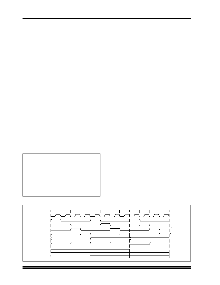
Clocking Scheme/Instruction
Cycle
The clock input (from OSC1) is internally divided by
four to generate four non-overlapping quadrature
clocks, namely Q1, Q2, Q3 and Q4. Internally, the
program counter (PC) is incremented every Q1, the
instruction is fetched from the program memory and
latched into the instruction register in Q4. The instruc-
tion is decoded and executed during the following Q1
through Q4. The clocks and instruction execution flow
are shown in Figure 4-4.
FIGURE 4-4:
CLOCK/INSTRUCTION CYCLE
CALL SUB1, FAST
;STATUS, WREG, BSR
;SAVED IN FAST REGISTER
;STACK
SUB1
RETURN FAST
;RESTORE VALUES SAVED
;IN FAST REGISTER STACK
Q1
Q2
Q3
Q4
Q1
Q2
Q3
Q4
Q1
Q2
Q3
Q4
OSC1
Q1
Q2
Q3
Q4
PC
OSC2/CLKO
(RC mode)
PC
PC+2
PC+4
Fetch INST (PC)
Execute INST (PC-2)
Fetch INST (PC+2)
Execute INST (PC)
Fetch INST (PC+4)
Execute INST (PC+2)
Internal
Phase
Clock
相关PDF资料 |
PDF描述 |
|---|---|
| PIC18LF4680T-I/ML | IC MCU FLASH 32KX16 44QFN |
| PIC18F23K22-I/MV | IC PIC MCU 8KB FLASH 28UQFN |
| PIC18F23K22-I/ML | IC PIC MCU 8KB FLASH 28QFN |
| PIC18LF4610T-I/ML | IC MCU FLASH 32KX16 44QFN |
| PIC16F882-I/ML | IC PIC MCU FLASH 2KX14 28QFN |
相关代理商/技术参数 |
参数描述 |
|---|---|
| PIC18LF6525-I/PT | 功能描述:8位微控制器 -MCU 48KB 3840 RAM 52I/O RoHS:否 制造商:Silicon Labs 核心:8051 处理器系列:C8051F39x 数据总线宽度:8 bit 最大时钟频率:50 MHz 程序存储器大小:16 KB 数据 RAM 大小:1 KB 片上 ADC:Yes 工作电源电压:1.8 V to 3.6 V 工作温度范围:- 40 C to + 105 C 封装 / 箱体:QFN-20 安装风格:SMD/SMT |
| PIC18LF6525T-I/PT | 功能描述:8位微控制器 -MCU 48KB 3840 RAM 52I/O RoHS:否 制造商:Silicon Labs 核心:8051 处理器系列:C8051F39x 数据总线宽度:8 bit 最大时钟频率:50 MHz 程序存储器大小:16 KB 数据 RAM 大小:1 KB 片上 ADC:Yes 工作电源电压:1.8 V to 3.6 V 工作温度范围:- 40 C to + 105 C 封装 / 箱体:QFN-20 安装风格:SMD/SMT |
| PIC18LF6527-I/PT | 功能描述:8位微控制器 -MCU 48 KB FL 4K RAM 70 I/O RoHS:否 制造商:Silicon Labs 核心:8051 处理器系列:C8051F39x 数据总线宽度:8 bit 最大时钟频率:50 MHz 程序存储器大小:16 KB 数据 RAM 大小:1 KB 片上 ADC:Yes 工作电源电压:1.8 V to 3.6 V 工作温度范围:- 40 C to + 105 C 封装 / 箱体:QFN-20 安装风格:SMD/SMT |
| PIC18LF6527-I/PT | 制造商:Microchip Technology Inc 功能描述:8-Bit Microcontroller IC |
| PIC18LF6527T-I/PT | 功能描述:8位微控制器 -MCU 48 KB FL 4K RAM 70 I/O RoHS:否 制造商:Silicon Labs 核心:8051 处理器系列:C8051F39x 数据总线宽度:8 bit 最大时钟频率:50 MHz 程序存储器大小:16 KB 数据 RAM 大小:1 KB 片上 ADC:Yes 工作电源电压:1.8 V to 3.6 V 工作温度范围:- 40 C to + 105 C 封装 / 箱体:QFN-20 安装风格:SMD/SMT |
发布紧急采购,3分钟左右您将得到回复。