- 您现在的位置:买卖IC网 > PDF目录11547 > PIC24FJ16GA002T-I/SO (Microchip Technology)IC PIC MCU FLASH 16K 28SOIC PDF资料下载
参数资料
| 型号: | PIC24FJ16GA002T-I/SO |
| 厂商: | Microchip Technology |
| 文件页数: | 28/52页 |
| 文件大小: | 0K |
| 描述: | IC PIC MCU FLASH 16K 28SOIC |
| 产品培训模块: | Graphics LCD System and PIC24 Interface Asynchronous Stimulus |
| 标准包装: | 1,600 |
| 系列: | PIC® 24F |
| 核心处理器: | PIC |
| 芯体尺寸: | 16-位 |
| 速度: | 32MHz |
| 连通性: | I²C,PMP,SPI,UART/USART |
| 外围设备: | 欠压检测/复位,LVD,POR,PWM,WDT |
| 输入/输出数: | 21 |
| 程序存储器容量: | 16KB(5.5K x 24) |
| 程序存储器类型: | 闪存 |
| RAM 容量: | 4K x 8 |
| 电压 - 电源 (Vcc/Vdd): | 2 V ~ 3.6 V |
| 数据转换器: | A/D 10x10b |
| 振荡器型: | 内部 |
| 工作温度: | -40°C ~ 85°C |
| 封装/外壳: | 28-SOIC(0.295",7.50mm 宽) |
| 包装: | 带卷 (TR) |
| 配用: | DM240011-ND - KIT STARTER MPLAB FOR PIC24F MCU AC162088-ND - HEADER MPLAB ICD2 24FJ64GA004 28 AC164339-ND - MODULE SKT FOR PM3 28SOIC DV164033-ND - KIT START EXPLORER 16 MPLAB ICD2 |
第1页第2页第3页第4页第5页第6页第7页第8页第9页第10页第11页第12页第13页第14页第15页第16页第17页第18页第19页第20页第21页第22页第23页第24页第25页第26页第27页当前第28页第29页第30页第31页第32页第33页第34页第35页第36页第37页第38页第39页第40页第41页第42页第43页第44页第45页第46页第47页第48页第49页第50页第51页第52页
PIC24FJXXXGA0XX
DS39768D-page 34
2008 Microchip Technology Inc.
5.0
THE PROGRAMMING
EXECUTIVE
5.1
Programming Executive
Communication
The programmer and programming executive have a
master-slave relationship, where the programmer is
the master programming device and the programming
executive is the slave.
All communication is initiated by the programmer in the
form of a command. Only one command at a time can
be sent to the programming executive. In turn, the
programming executive only sends one response to
the programmer after receiving and processing a
command. The programming executive command set
is described in Section 5.2 “Programming Executive
Commands”. The response set is described in
5.1.1
COMMUNICATION INTERFACE
AND PROTOCOL
The Enhanced ICSP interface is a 2-wire SPI,
implemented using the PGCx and PGDx pins. The
PGCx pin is used as a clock input pin and the clock
source must be provided by the programmer. The
PGDx pin is used for sending command data to, and
receiving response data from, the programming
executive.
Data transmits to the device must change on the rising
edge and hold on the falling edge. Data receives from
the device must change on the falling edge and hold on
the rising edge.
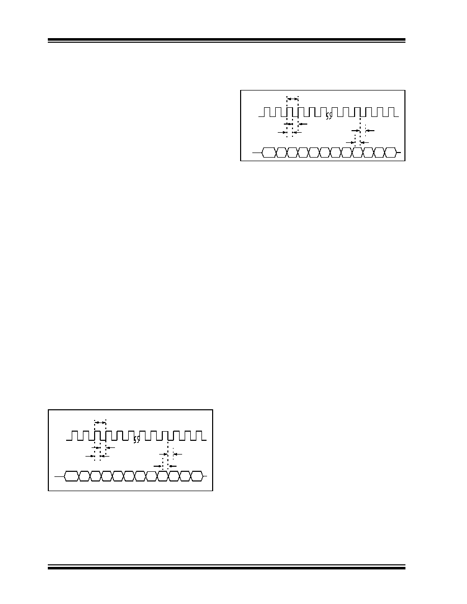
All data transmissions are sent to the Most Significant
bit (MSb) first, using 16-bit mode (see Figure 5-1).
FIGURE 5-1:
PROGRAMMING
EXECUTIVE SERIAL
TIMING FOR DATA
RECEIVED FROM DEVICE
FIGURE 5-2:
PROGRAMMING
EXECUTIVE SERIAL TIMING
FOR DATA TRANSMITTED
TO DEVICE
Since a 2-wire SPI is used, and data transmissions are
half duplex, a simple protocol is used to control the
direction of PGDx. When the programmer completes a
command transmission, it releases the PGDx line and
allows the programming executive to drive this line
high. The programming executive keeps the PGDx line
high to indicate that it is processing the command.
After the programming executive has processed the
command, it brings PGDx low for 15
μsec to indicate to
the programmer that the response is available to be
clocked out. The programmer can begin to clock out the
response 23
μsec after PGDx is brought low, and it must
provide the necessary amount of clock pulses to receive
the entire response from the programming executive.
After the entire response is clocked out, the program-
mer should terminate the clock on PGCx until it is time
to send another command to the programming
executive. This protocol is shown in Figure 5-3.
5.1.2
SPI RATE
In Enhanced ICSP mode, the PIC24FJXXXGA0XX
family devices operate from the internal Fast RC oscil-
lator (FRCDIV), which has a nominal frequency of
8 MHz. This oscillator frequency yields an effective
system clock frequency of 4 MHz. To ensure that the
programmer does not clock too fast, it is recommended
that a 4 MHz clock be provided by the programmer.
5.1.3
TIME-OUTS
The programming executive uses no Watchdog Timer
or time-out for transmitting responses to the program-
mer. If the programmer does not follow the flow control
mechanism using PGCx, as described in Section 5.1.1
possible that the programming executive will behave
unexpectedly while trying to send a response to the
programmer. Since the programming executive has no
time-out, it is imperative that the programmer correctly
follow the described communication protocol.
As a safety measure, the programmer should use the
command time-outs identified in Table 5-1. If the
command time-out expires, the programmer should
reset
the
programming
executive
and
start
programming the device again.
PGCx
PGDx
12
3
11
13
15
16
14
12
LSb
14
13
12
11
45
6
MSb
1
2
3
...
4
5
P2
P3
P1
P1B
P1A
PGCx
PGDx
12
3
11
13
15
16
14
12
LSb
14
13 12
11
45
6
MSb
1
2
3
...
4
5
P2
P3
P1
P1B
P1A
相关PDF资料 |
PDF描述 |
|---|---|
| GJM0335C1E1R8BB01D | CAP CER 1.8PF 25V NP0 0201 |
| GJM0335C1ER40BB01D | CAP CER 0.4PF 25V NP0 0201 |
| V375C12M75BF2 | CONVERTER MOD DC/DC 12V 75W |
| V375C12M75B3 | CONVERTER MOD DC/DC 12V 75W |
| GJM0335C1ER30BB01D | CAP CER 0.3PF 25V NP0 0201 |
相关代理商/技术参数 |
参数描述 |
|---|---|
| PIC24FJ16GA004 | 制造商:MICROCHIP 制造商全称:Microchip Technology 功能描述:PIC24FJ64GA004 Family Silicon Errata and Data Sheet Clarification |
| PIC24FJ16GA004-E/ML | 功能描述:16位微控制器 - MCU 16B 16KB Flash I/O 16 MIPS nanoWatt RoHS:否 制造商:Texas Instruments 核心:RISC 处理器系列:MSP430FR572x 数据总线宽度:16 bit 最大时钟频率:24 MHz 程序存储器大小:8 KB 数据 RAM 大小:1 KB 片上 ADC:Yes 工作电源电压:2 V to 3.6 V 工作温度范围:- 40 C to + 85 C 封装 / 箱体:VQFN-40 安装风格:SMD/SMT |
| PIC24FJ16GA004-E/PT | 功能描述:16位微控制器 - MCU 16B 16KB Flash I/O 16 MIPS nanoWatt RoHS:否 制造商:Texas Instruments 核心:RISC 处理器系列:MSP430FR572x 数据总线宽度:16 bit 最大时钟频率:24 MHz 程序存储器大小:8 KB 数据 RAM 大小:1 KB 片上 ADC:Yes 工作电源电压:2 V to 3.6 V 工作温度范围:- 40 C to + 85 C 封装 / 箱体:VQFN-40 安装风格:SMD/SMT |
| PIC24FJ16GA004-EPT | 制造商:MICROCHIP 制造商全称:Microchip Technology 功能描述:PIC24FJXXXGA0XX Flash Programming Specification |
| PIC24FJ16GA004-I/ML | 功能描述:16位微控制器 - MCU 16b Fam 16MIPS 16KB FL 4096b RAM 35 I/O RoHS:否 制造商:Texas Instruments 核心:RISC 处理器系列:MSP430FR572x 数据总线宽度:16 bit 最大时钟频率:24 MHz 程序存储器大小:8 KB 数据 RAM 大小:1 KB 片上 ADC:Yes 工作电源电压:2 V to 3.6 V 工作温度范围:- 40 C to + 85 C 封装 / 箱体:VQFN-40 安装风格:SMD/SMT |
发布紧急采购,3分钟左右您将得到回复。