- 您现在的位置:买卖IC网 > PDF目录11465 > PIC24HJ32GP204T-I/PT (Microchip Technology)IC PIC MCU FLASH 32K 44TQFP PDF资料下载
参数资料
| 型号: | PIC24HJ32GP204T-I/PT |
| 厂商: | Microchip Technology |
| 文件页数: | 77/289页 |
| 文件大小: | 0K |
| 描述: | IC PIC MCU FLASH 32K 44TQFP |
| 产品培训模块: | Asynchronous Stimulus |
| 标准包装: | 1,200 |
| 系列: | PIC® 24H |
| 核心处理器: | PIC |
| 芯体尺寸: | 16-位 |
| 速度: | 40 MIP |
| 连通性: | I²C,IrDA,LIN,SPI,UART/USART |
| 外围设备: | 欠压检测/复位,POR,PWM,WDT |
| 输入/输出数: | 35 |
| 程序存储器容量: | 32KB(11K x 24) |
| 程序存储器类型: | 闪存 |
| RAM 容量: | 2K x 8 |
| 电压 - 电源 (Vcc/Vdd): | 3 V ~ 3.6 V |
| 数据转换器: | A/D 13x10b/12b |
| 振荡器型: | 内部 |
| 工作温度: | -40°C ~ 85°C |
| 封装/外壳: | 44-TQFP |
| 包装: | 带卷 (TR) |
| 配用: | DM240001-ND - BOARD DEMO PIC24/DSPIC33/PIC32 |
| 其它名称: | PIC24HJ32GP204T-I/PTTR |
第1页第2页第3页第4页第5页第6页第7页第8页第9页第10页第11页第12页第13页第14页第15页第16页第17页第18页第19页第20页第21页第22页第23页第24页第25页第26页第27页第28页第29页第30页第31页第32页第33页第34页第35页第36页第37页第38页第39页第40页第41页第42页第43页第44页第45页第46页第47页第48页第49页第50页第51页第52页第53页第54页第55页第56页第57页第58页第59页第60页第61页第62页第63页第64页第65页第66页第67页第68页第69页第70页第71页第72页第73页第74页第75页第76页当前第77页第78页第79页第80页第81页第82页第83页第84页第85页第86页第87页第88页第89页第90页第91页第92页第93页第94页第95页第96页第97页第98页第99页第100页第101页第102页第103页第104页第105页第106页第107页第108页第109页第110页第111页第112页第113页第114页第115页第116页第117页第118页第119页第120页第121页第122页第123页第124页第125页第126页第127页第128页第129页第130页第131页第132页第133页第134页第135页第136页第137页第138页第139页第140页第141页第142页第143页第144页第145页第146页第147页第148页第149页第150页第151页第152页第153页第154页第155页第156页第157页第158页第159页第160页第161页第162页第163页第164页第165页第166页第167页第168页第169页第170页第171页第172页第173页第174页第175页第176页第177页第178页第179页第180页第181页第182页第183页第184页第185页第186页第187页第188页第189页第190页第191页第192页第193页第194页第195页第196页第197页第198页第199页第200页第201页第202页第203页第204页第205页第206页第207页第208页第209页第210页第211页第212页第213页第214页第215页第216页第217页第218页第219页第220页第221页第222页第223页第224页第225页第226页第227页第228页第229页第230页第231页第232页第233页第234页第235页第236页第237页第238页第239页第240页第241页第242页第243页第244页第245页第246页第247页第248页第249页第250页第251页第252页第253页第254页第255页第256页第257页第258页第259页第260页第261页第262页第263页第264页第265页第266页第267页第268页第269页第270页第271页第272页第273页第274页第275页第276页第277页第278页第279页第280页第281页第282页第283页第284页第285页第286页第287页第288页第289页
PIC24HJ32GP202/204 AND PIC24HJ16GP304
DS70289J-page 168
2007-2011 Microchip Technology Inc.
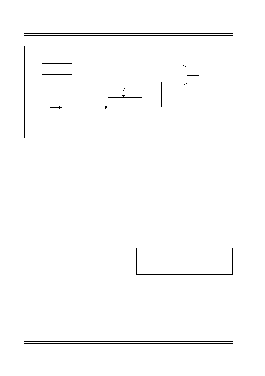
FIGURE 18-3:
ADC CONVERSION CLOCK PERIOD BLOCK DIAGRAM
18.3
ADC Helpful Tips
1.
The SMPI<3:0> (AD1CON2<5:2>) control bits:
a) Determine when the ADC interrupt flag is
set and an interrupt is generated if enabled.
b) When the CSCNA bit (AD1CON2<10>) is
set to ‘1’, determines when the ADC analog
scan
channel
list
defined
in
the
AD1CSSL/AD1CSSH registers starts over
from the beginning.
c)
On devices without a DMA peripheral,
determines when ADC result buffer pointer
to ADC1BUF0-ADC1BUFF, gets reset back
to the beginning at ADC1BUF0.
2.
On devices without a DMA module, the ADC has
16 result buffers. ADC conversion results are
stored sequentially in ADC1BUF0-ADC1BUFF
regardless of which analog inputs are being
used
subject
to
the
SMPI<3:0>
bits
(AD1CON2<5:2>) and the condition described
in 1c above. There is no relationship between
the ANx input being measured and which ADC
buffer
(ADC1BUF0-ADC1BUFF)
that
the
conversion results will be placed in.
3.
On devices with a DMA module, the ADC mod-
ule has only 1 ADC result buffer, (i.e.,
ADC1BUF0), per ADC peripheral and the ADC
conversion result must be read either by the
CPU or DMA controller before the next ADC
conversion is complete to avoid overwriting the
previous value.
4.
The DONE bit (AD1CON1<0>) is only cleared at
the start of each conversion and is set at the
completion of the conversion, but remains set
indefinitely even through the next sample phase
until the next conversion begins. If application
code is monitoring the DONE bit in any kind of
software loop, the user must consider this
behavior because the CPU code execution is
faster than the ADC. As a result, in manual sam-
ple mode, particularly where the users code is
setting the SAMP bit (AD1CON1<1>), the
DONE bit should also be cleared by the user
application just before setting the SAMP bit.
5.
On devices with two ADC modules, the
ADCxPCFG registers for both ADC modules
must be set to a logic ‘1’ to configure a target
I/O pin as a digital I/O pin. Failure to do so
means that any alternate digital input function
will always see only a logic ‘0’ as the digital
input buffer is held in Disable mode.
18.4
ADC Resources
Many useful resources are provided on the main prod-
uct page of the Microchip web site for the devices listed
in this data sheet. This product page, which can be
accessed using this link, contains the latest updates
and additional information.
18.4.1
KEY RESOURCES
Section 16. “Analog-to-Digital Converter
(ADC)”
(DS70183)
Code Samples
Application Notes
Software Libraries
Webinars
All related dsPIC33F/PIC24H Family Reference
Manuals Sections
Development Tools
0
1
ADC Internal
RC Clock(2)
TOSC(1)
X
2
ADC Conversion
Clock Multiplier
1, 2, 3, 4, 5,..., 64
AD1CON3<15>
TCY
TAD
6
AD1CON3<5:0>
Note 1:
Refer to Figure 8-2 for the derivation of FOSC when the PLL is enabled. If the PLL is not used, FOSC is equal
to the clock frequency. TOSC = 1/FOSC.
2:
See the ADC Electrical Characteristics for the exact RC Clock value.
Note:
In the event you are not able to access
the product page using the link above,
enter
this
URL
in
your
browser:
相关PDF资料 |
PDF描述 |
|---|---|
| GRM2196S2A1R0CD01D | CAP CER 1PF 100V S2H 0805 |
| GRM2196R2A4R7CD01D | CAP CER 4.7PF 100V R2H 0805 |
| GRM2196R2A4R3CD01D | CAP CER 4.3PF 100V R2H 0805 |
| GRM2196R2A3R9CD01D | CAP CER 3.9PF 100V R2H 0805 |
| GRM2196R2A3R3CD01D | CAP CER 3.3PF 100V R2H 0805 |
相关代理商/技术参数 |
参数描述 |
|---|---|
| PIC24HJ32GP302 | 制造商:MICROCHIP 制造商全称:Microchip Technology 功能描述:High-Performance, 16-bit Microcontrollers |
| PIC24HJ32GP302_11 | 制造商:MICROCHIP 制造商全称:Microchip Technology 功能描述:High-Performance, 16-bit Microcontrollers |
| PIC24HJ32GP302-E/ML | 制造商:MICROCHIP 制造商全称:Microchip Technology 功能描述:High-Performance, 16-bit Microcontrollers |
| PIC24HJ32GP302-E/MM | 功能描述:16位微控制器 - MCU 16 Bit MCU 40MIPS 32 KB FLASH RoHS:否 制造商:Texas Instruments 核心:RISC 处理器系列:MSP430FR572x 数据总线宽度:16 bit 最大时钟频率:24 MHz 程序存储器大小:8 KB 数据 RAM 大小:1 KB 片上 ADC:Yes 工作电源电压:2 V to 3.6 V 工作温度范围:- 40 C to + 85 C 封装 / 箱体:VQFN-40 安装风格:SMD/SMT |
| PIC24HJ32GP302-E/PT | 制造商:MICROCHIP 制造商全称:Microchip Technology 功能描述:High-Performance, 16-bit Microcontrollers |
发布紧急采购,3分钟左右您将得到回复。