- 您现在的位置:买卖IC网 > PDF目录98053 > PKD4510ASI (ERICSSON POWER MODULES AB) 1-OUTPUT 50 W DC-DC REG PWR SUPPLY MODULE PDF资料下载
参数资料
| 型号: | PKD4510ASI |
| 厂商: | ERICSSON POWER MODULES AB |
| 元件分类: | 电源模块 |
| 英文描述: | 1-OUTPUT 50 W DC-DC REG PWR SUPPLY MODULE |
| 封装: | ROHS COMPLIANT, SMD-24 |
| 文件页数: | 8/18页 |
| 文件大小: | 570K |
| 代理商: | PKD4510ASI |
Ericsson Internal
PRODUCT SPECIFICATION
2 (5)
Prepared (also subject responsible if other)
No.
MICUPEZ
4/1301-BMR 622 Uen
Approved
Checked
Date
Rev
Reference
M. Anderzen
See § 1
2006-03-14
B
Soldering Information - Surface mounting
The product is intended for convection or vapor phase reflow
SnPb [and/or] Pb-free processes. To achieve a good and
reliable soldering result, make sure to follow the
recommendations from the solder paste supplier, to use
state-of-the-art reflow equipment and reflow profiling
techniques as well as the following guidelines.
A no-clean flux is recommended to avoid entrapment of
cleaning fluids in cavities inside the product. The cleaning
residues may affect long time reliability and isolation voltage.
A sufficiently extended preheat time is recommended to
ensure an even temperature across the host PCB, for both
small and large devices. To reduce the risk of excessive
heating is also recommended to reduce the time in the reflow
zone as much as possible.
Minimum pin temperature recommendations
Pin number 22 is chosen as reference location for the
minimum pin temperature recommendations.
SnPb solder processes
For Pb solder processes, a pin temperature (T
PIN) in excess of
the solder melting temperature, (T
L, +183°C for Sn63/Pb37)
for more than 30 seconds, and a peak temperature of +210°C
is recommended to ensure a reliable solder joint.
Lead-free (Pb-free) solder processes
For Pb-free solder processes, a pin temperature (T
PIN) in
excess of the solder melting temperature (T
L, +217 to +221 °C
for Sn/Ag/Cu solder alloys) for more than 30 seconds, and a
peak temperature of +235°C on all solder joints is
recommended to ensure a reliable solder joint.
SnPb solder processes
For conventional SnPb solder processes, the product is
qualified for MSL 1 according to IPC/JEDEC standard
J-STD-020C.
During reflow, T
Pin must not exceed +235 °C at any time.
Min 10 s over 200 °C
30-100 s over 183 °C
Lead-free (Pb-free) solder processes- TBD AFTER REVIEW
For Pb-free solder processes, the product is qualified for
MSL 1 according to IPC/JEDEC standard J-STD-020C.
During reflow, T
Pin must not exceed +260 °C at any time.
max 20 s over 230 °C
30-100 s over 221 °C
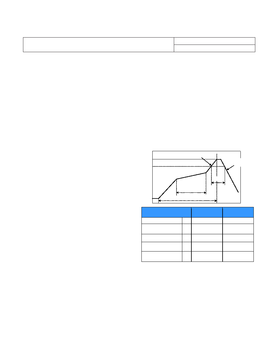
25 °C
Time
Temperature
Ramp-down
(cooling)
Ramp-up
Reflow
Preheat
Time 25 °C to peak
T
P
T
L
Profile features
Sn/Pb eutectic
assembly
Pb-free assembly
Average ramp-up rate
3 °C/s max
Solder melting
temperature (typical)
T
L
+183 °C
+221 °C
Peak product temperature T
P
+235 °C
+260 °C
Average ramp-down rate
4 °C/s max
Time 25 °C to peak
temperature
6 minutes max
8 minutes max
E
PKD 4000 ASI series
DC/DC converters, Input 36-75 V, Output 20 A/50 W
EN/LZT 146 346 R1A April 2006
Ericsson Power Modules AB
Technical Specication
16
相关PDF资料 |
PDF描述 |
|---|---|
| PKD4218LASI | 1-OUTPUT 24.2 W DC-DC REG PWR SUPPLY MODULE |
| PKD4510ESI | 1-OUTPUT 50 W DC-DC REG PWR SUPPLY MODULE |
| PKD4218HESPBI | 1-OUTPUT 21 W DC-DC REG PWR SUPPLY MODULE |
| PKD4510ESPBI | 1-OUTPUT 50 W DC-DC REG PWR SUPPLY MODULE |
| PKD4218LESPBI | 1-OUTPUT 24 W DC-DC REG PWR SUPPLY MODULE |
相关代理商/技术参数 |
参数描述 |
|---|---|
| PKD4510ESI | 功能描述:DC/DC转换器 3.3 Vdc 15A Iso Input 36-75V 50W RoHS:否 制造商:Murata 产品: 输出功率: 输入电压范围:3.6 V to 5.5 V 输入电压(标称): 输出端数量:1 输出电压(通道 1):3.3 V 输出电流(通道 1):600 mA 输出电压(通道 2): 输出电流(通道 2): 安装风格:SMD/SMT 封装 / 箱体尺寸: |
| PKD480 | 制造商:Pyle 功能描述:1 Diameter 200W Max Tweeter Dynamic Horn 制造商:PYLE 功能描述:TWEETER DYNAMIC HORN 1 DIAMETER 200W MAX |
| PKD60B1/4 | 功能描述:旋钮和转盘 STRGHT 0.8" W/SKIRT SWITCH KNOB RoHS:否 制造商:Davies Molding 材料:Phenolic 设计:Set Screw 轴尺寸:0.25 in 直径:3/4 in 颜色:Black 指示器型式:Line |
| PKD60B1/8 | 功能描述:旋钮和转盘 STRGHT 0.8" W/SKIRT SWITCH KNOB RoHS:否 制造商:Davies Molding 材料:Phenolic 设计:Set Screw 轴尺寸:0.25 in 直径:3/4 in 颜色:Black 指示器型式:Line |
| PKD60B101/4 | 制造商:TE Connectivity 功能描述:Switch Access Rotary Switch Round Knob |
发布紧急采购,3分钟左右您将得到回复。