- 您现在的位置:买卖IC网 > PDF目录378055 > PM5945-UTP5 (PMC-Sierra, Inc.) ATM PHYSICAL INTERFACE APPLICATION BOARD FOR CAT-5 UTP PDF资料下载
参数资料
| 型号: | PM5945-UTP5 |
| 厂商: | PMC-Sierra, Inc. |
| 英文描述: | ATM PHYSICAL INTERFACE APPLICATION BOARD FOR CAT-5 UTP |
| 中文描述: | ATM物理接口猫应用板- 5双绞线 |
| 文件页数: | 9/84页 |
| 文件大小: | 1666K |
| 代理商: | PM5945-UTP5 |
第1页第2页第3页第4页第5页第6页第7页第8页当前第9页第10页第11页第12页第13页第14页第15页第16页第17页第18页第19页第20页第21页第22页第23页第24页第25页第26页第27页第28页第29页第30页第31页第32页第33页第34页第35页第36页第37页第38页第39页第40页第41页第42页第43页第44页第45页第46页第47页第48页第49页第50页第51页第52页第53页第54页第55页第56页第57页第58页第59页第60页第61页第62页第63页第64页第65页第66页第67页第68页第69页第70页第71页第72页第73页第74页第75页第76页第77页第78页第79页第80页第81页第82页第83页第84页
S
TANDARD
P
RODUCT
PMC-Sierra, Inc.
PM5945 -UTP5
PMC-940202 ISSUE 2. APRIL 7, 1995
______________________________________________________________________________________________
APP_SAPI_UTP5
______________________________________________________________________________________________
5
mode of operation on the receive side of the S/UNI device. In the normal mode of
operation (good incoming signal) the S/UNI device is in the serial mode and accepts
clock and data from the high speed interface (RSER is high). In loss of signal
condition, the S/UNI device is switched to the parallel mode and accepts data from
the PICLK and PIN[7:0] inputs. The POCLK is switched to generate the 19.44 MHz
PICLK. This technique also guarantees that the S/UNI will generate a LOS
indication when the TWISTER loses incoming signal. This is achieved due to the
CY7B951 not squelching the data in a loss of signal condition.
The transmit line interface consists of the S/UNI PECL transmit outputs that are
buffered by the CY7B951 and then connected to the TWISTER's transmit section.
Outgoing data on TXO+/- pins is coupled to the line via a 1:1 turns ratio transformer.
The receive line interface consists of a 1:1.4 step-up transformer coupling data from
the UTP5 cables to the RXI+/- pins of the TWISTER. The received datastream is
equalized and output by the TWISTER to the CY7B951 which recovers the data and
clock and relays the them to the S/UNI via its PECL differential outputs.
An 8 pin 8 position RJ45 modular jack is used to connect to the UTP5 cables. The
unused pairs of cables are terminated via a resistor network to a common mode
termination point. The center taps of the transformers are also terminated to the
same point.
The S/UNI is configured for bit serial operation. The 155.52 MHz transmit clock
source is synthesized by the CY7B951 from a 19.44 MHz oscillator. The receive
clock and data recovery is supplied by the Cypress CY7B951 device. If the loop
back select is enabled on the CY7B951 the transmit data is muxed into the receive
PLL and the recovered clock and data are fed back to the S/UNI device. The S/UNI
can also be configured for loop time operation. When configured for loop time
operation, only a receive clock and data recovery device is required.
UTOPIA Identification ROM
The upper 32 bytes of the address space is used by the UTOPIA identification ROM
to hold the interface configuration information.
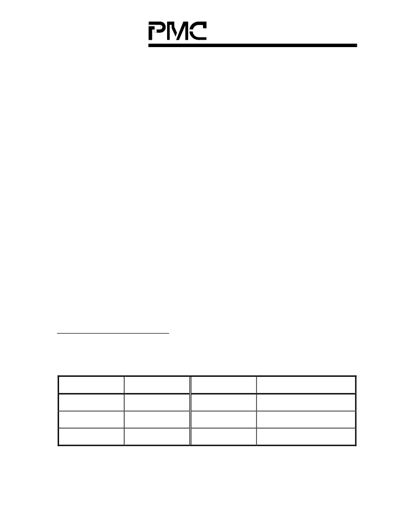
Table 1: Standard ROM Address and Content
Address
Function
Address
Function
0x1E0
Protocol Type
0x1E4-0x1EB
64 or 48-bit Address
0x1E1
Media Type
0x1EC-0x1EF
Reserved
0x1E2-0x1E3
Capability
0x1F0-0x1FF
Manufacturer ID, Version
相关PDF资料 |
PDF描述 |
|---|---|
| PM5945 | CONN |
| PM6341 | E1 TRANSCEIVER |
| PM6341-QI | Ultraframer DS3/E3/DS2/E2/DS1/E1/DS0 |
| PM6341-RI | Ultraframer DS3/E3/DS2/E2/DS1/E1/DS0 |
| PM6344-RI | KPSE SERIES |
相关代理商/技术参数 |
参数描述 |
|---|---|
| PM594D | 制造商:未知厂家 制造商全称:未知厂家 功能描述:Analog IC |
| PM594DS | 制造商:未知厂家 制造商全称:未知厂家 功能描述:Analog IC |
| PM594K | 制造商:未知厂家 制造商全称:未知厂家 功能描述:Analog IC |
| PM594KS | 制造商:未知厂家 制造商全称:未知厂家 功能描述:Analog IC |
| PM594S | 制造商:未知厂家 制造商全称:未知厂家 功能描述:Analog IC |
发布紧急采购,3分钟左右您将得到回复。