- 您现在的位置:买卖IC网 > PDF目录97636 > PS12014-A AC MOTOR CONTROLLER, 20 A, XMA29 PDF资料下载
参数资料
| 型号: | PS12014-A |
| 元件分类: | 运动控制电子 |
| 英文描述: | AC MOTOR CONTROLLER, 20 A, XMA29 |
| 文件页数: | 2/6页 |
| 文件大小: | 395K |
| 代理商: | PS12014-A |
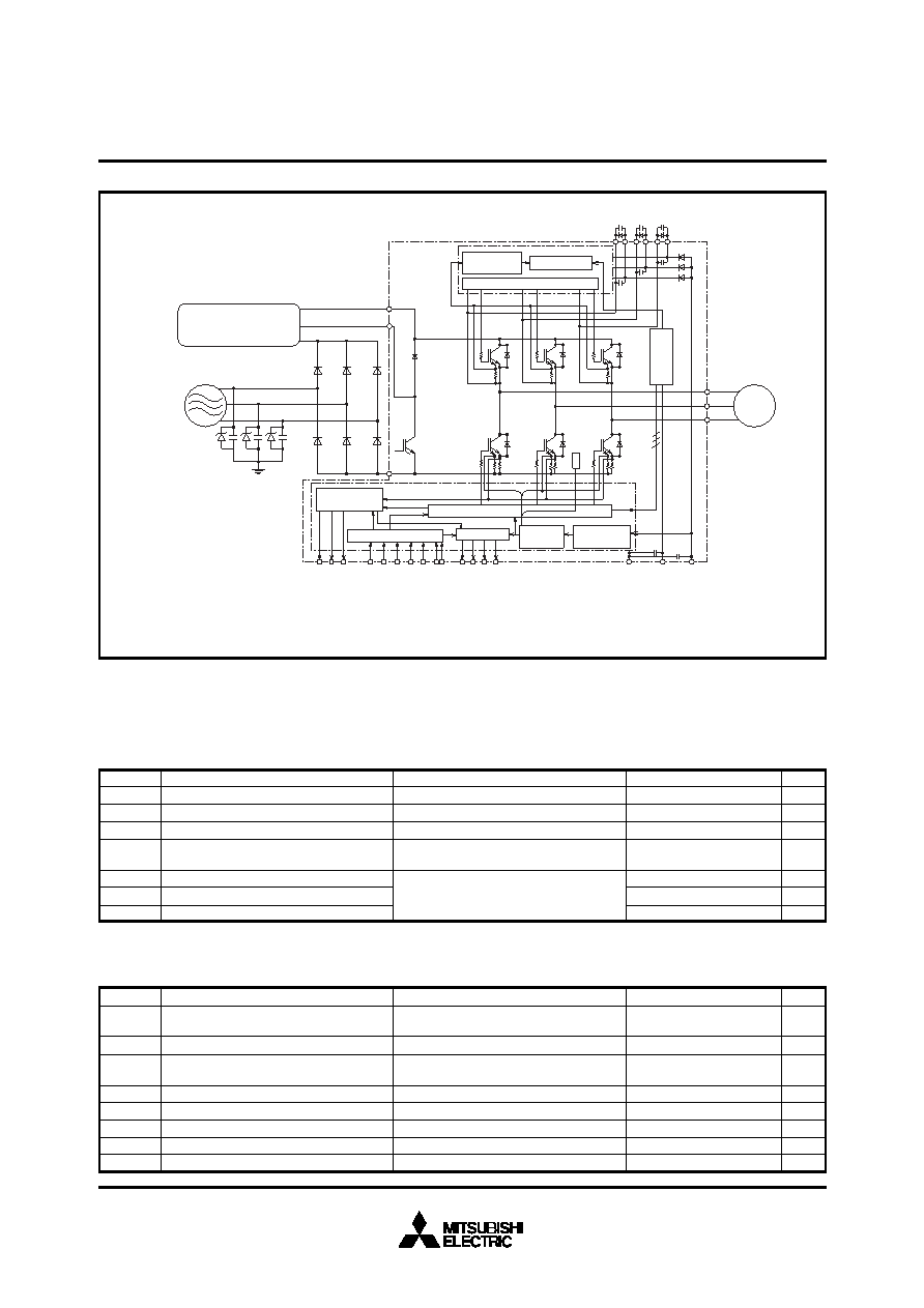
MITSUBISHI SEMICONDUCTOR <Application Specific Intelligent Power Module>
PS12014-A
FLAT-BASE TYPE
INSULATED TYPE
Jan. 2000
CBU–
CBU+
CBV–
CBV+
CBW–
CBW+
GND
VDL VDH
Fo Logic
Application Specific Intelligent
Power Module
CU CV CW
CL,FO1,FO2,FO3
UP VP WP
VN WN Br
UN
B
P
Protection
Circuit
Photo
Coupler
Input Circuit
Drive Circuit
Input signal conditioning
Current sensing
circuit
Protection
circuit
Control supply
fault sense
R
S
T
Z : Surge absorber.
C : AC filter (Ceramic condenser 2.2~6.5nF)
[Note : Additionally an appropriate Line-to line
surge absorber circuit may become necessary
depending on the application environment].
C
Z
N
M
W
AC 400V class
line output
V
U
Brake resistor connection,
AC 400V class line input
Inrush prevention circuit,
etc.
T
S
Analogue signal output corresponding to
each phase current (5V line) Note 1)
PWM input
(5V line) Note 2)
Note 1) To prevent chances of signal oscillation, a series resistor (1k
) coupling at each output is recommended.
Note 2) By virtue of integrating a photo-coupler inside the module, direct coupling to CPU, without any extemal opto or transformer isolation is possible.
Note 3) All outputs are open collector type. Each signal line should be pulled up to plus side of the 5V power supply with approximately 5.1k
resistance.
Note 4) The wiring between power DC link capacitor and P/N terminals should be as short as possible to protect the ASIPM against catastrophic high surge voltage.
For extra precaution, a small film snubber capacitor (0.1~0.22
F, high voltage type) is recommended to be mounted close to these P and N DC power input pins.
Fault output
(5V line) Note 3)
INTERNAL FUNCTIONS BLOCK DIAGRAM
(Fig. 2)
±Ic(±Icp)
Ic(Icp)
IF(IFP)
V
900
1000
1200
Applied between P-N
Applied between P-N, Surge-value
Applied between P-U, V, W, Br or U, V, W, Br-N
Supply voltage
Supply voltage (surge)
Each output IGBT collector-emitter static voltage
Condition
Symbol
Item
Ratings
Unit
VCC
VCC(surge)
VP or VN
MAXIMUM RATINGS (Tj = 25
°C)
INVERTER PART (Including Brake Part)
VP(S) or
VN(S)
Each output IGBT collector-emitter surge voltage
Each output IGBT collector current
Brake IGBT collector current
Brake diode anode current
Applied between P-U, V, W, Br or U, V, W, Br-N
TC = 25
°C
Note : “(
)” means IC peak value
1200
±10 (±20)
5 (10)
V
A
VCIN
VFO
IFO
VCL
ICL
ICO
V
7
Applied between VDL-GND
Supply voltage
VDL
Symbol
Item
Ratings
Unit
CONTROL PART
Condition
Input signal voltage
Fault output supply voltage
Fault output current
Current-limit warning output voltage
CL output current
Analogue-current-signal output current
–0.5 ~ VDL+0.5
V
mA
V
mA
Applied between UP VP WP UN VN
WN Br-GND
Applied between FO1 FO2 FO3-GND
Sink current of FO1 FO2 FO3
Applied between CL-GND
Sink current of CL
Sink current of CU CV CW
–0.5 ~ 7
15
–0.5 ~ 7
15
±1
VDH, VDB
Supply voltage
V
20
Applied between VDH-GND, CBU+-CBU–,
CBV+-CBV–, CBW+-CBW–
相关PDF资料 |
PDF描述 |
|---|---|
| PS21444-E | AC MOTOR CONTROLLER, 30 A, DMA26 |
| PS21543-G | AC MOTOR CONTROLLER, 20 A, DMA35 |
| PS21562-SP | AC MOTOR CONTROLLER, 10 A, XMA37 |
| PS21562 | AC MOTOR CONTROLLER, 10 A, XMA35 |
| PS21563-P | AC MOTOR CONTROLLER, 20 A, DMA35 |
相关代理商/技术参数 |
参数描述 |
|---|---|
| PS12015 | 制造商:POWEREX 制造商全称:Powerex Power Semiconductors 功能描述:FLAT-BASE TYPE INSULATED TYPE |
| PS120-15 | 制造商:Banner Engineering 功能描述:Power Supply, 120VAC Input, 15VDC @ 1 Amp Output, 8 Pin Octal Socket Connection |
| PS12015-A | 功能描述:MOD IPM 3PHASE IGBT 1200V 15A RoHS:否 类别:半导体模块 >> 功率驱动器 系列:- 标准包装:15 系列:SPM® 类型:FET 配置:三相反相器 电流:1.8A 电压:500V 电压 - 隔离:1500Vrms 封装/外壳:23-DIP 模块 |
| PS12017-A | 功能描述:MOD IPM 3PHASE IGBT 1200V 25A RoHS:否 类别:半导体模块 >> 功率驱动器 系列:- 标准包装:15 系列:SPM® 类型:FET 配置:三相反相器 电流:1.8A 电压:500V 电压 - 隔离:1500Vrms 封装/外壳:23-DIP 模块 |
| PS12018-A | 功能描述:MOD IPM 3PHASE IGBT 1200V 25A RoHS:否 类别:半导体模块 >> 功率驱动器 系列:- 标准包装:15 系列:SPM® 类型:FET 配置:三相反相器 电流:1.8A 电压:500V 电压 - 隔离:1500Vrms 封装/外壳:23-DIP 模块 |
发布紧急采购,3分钟左右您将得到回复。