- 您现在的位置:买卖IC网 > PDF目录96751 > PS12017-A AC MOTOR CONTROLLER, 50 A, UFM36 PDF资料下载
参数资料
| 型号: | PS12017-A |
| 元件分类: | 运动控制电子 |
| 英文描述: | AC MOTOR CONTROLLER, 50 A, UFM36 |
| 文件页数: | 4/6页 |
| 文件大小: | 397K |
| 代理商: | PS12017-A |
MITSUBISHI SEMICONDUCTOR <Application Specific Intelligent Power Module>
PS12017-A
FLAT-BASE TYPE
INSULATED TYPE
Jan. 2000
PRELIMINARY
Notice:
This
is not
a final
specification.
Some
parametric
limits
are subject
to change.
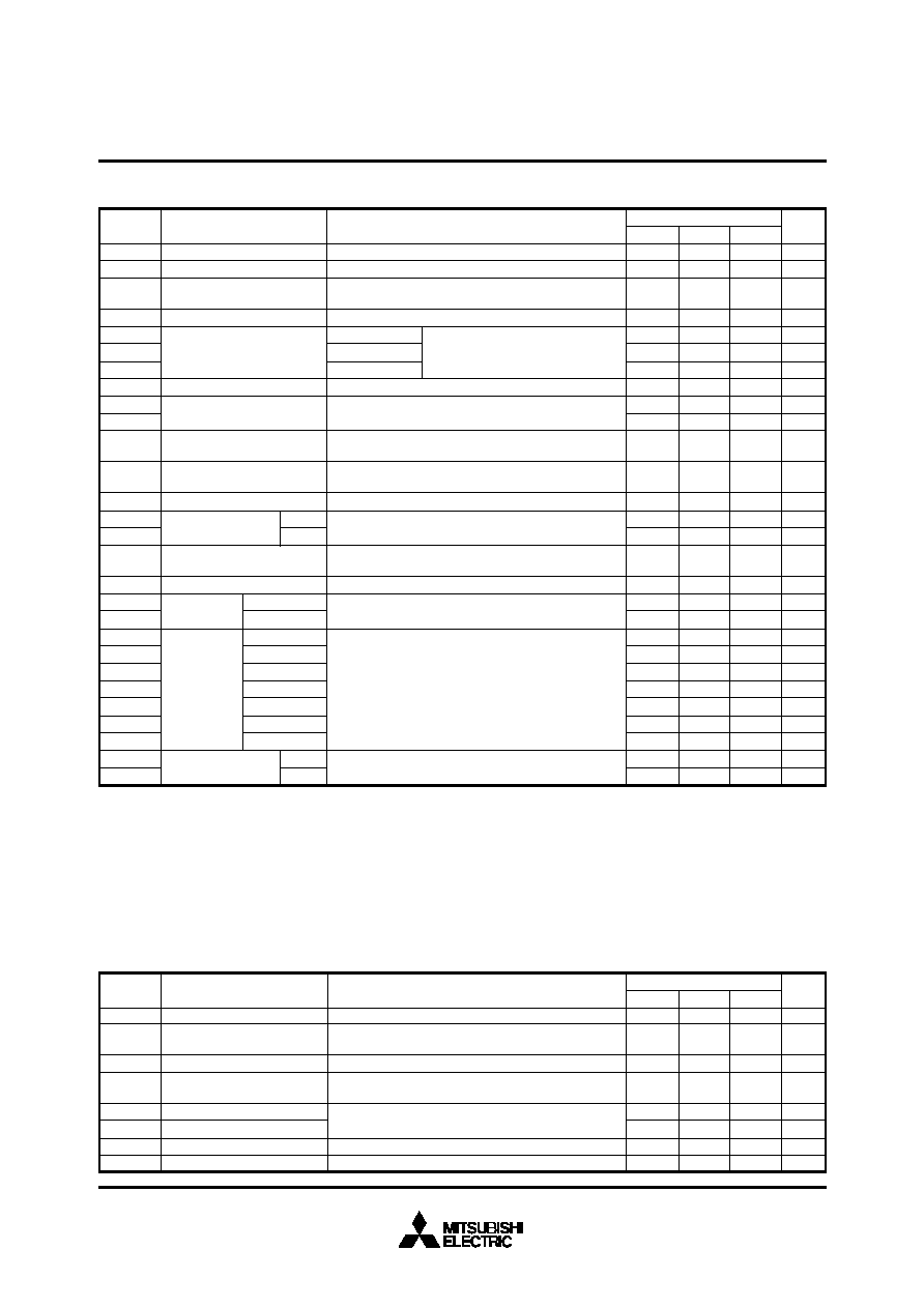
ELECTRICAL CHARACTERISTICS (Tj = 25
°C, VDH = 15V, VDB = 15V, VDL = 5V unless otherwise noted)
(Note 3) : (a) Allowable minimum input on-pulse width : This item applies to P-side circuit only.
(b) Allowable maximum input on-pulse width : This item applies to both P-side and N-side circuits excluding the brake circuit.
(Note4) : CL output : The "current limit warning (CL) operation circuit outputs warning signal whenever the arm current exceeds this limit. The
circuit is reset automatically by the next input signal and thus, it operates on a pulse-by-pulse scheme.
(Note5) : The short circuit protection works instantaneously when a high short circuit current flows through an internal IGBT rising up momen-
tarily. The protection function is, thus meant primarily to protect the ASIPM against short circuit distraction. Therefore, this function is
not recommended to be used for any system load current regulation or any over load control as this might, cause a failure due to
excessive temperature rise. Instead, the analogue current output feature or the over load warning feature (CL) should be appropri-
ately used for such current regulation or over load control operation. In other words, the PWM signals to the ASIPM should be shut
down, in principle, and not to be restarted before the junction temperature would recover to normal, as soon as a fault is feed back
from its FO1 pin of the ASIPM indicating a short circuit situation.
SC
OT
OTr
UVDB
UVDBr
UVDH
UVDHr
OVDH
OVDHr
tdv
IFO(H)
IFO(L)
±IOL
VDL = 5V, VDH = 15V, TC = –20 ~ 100
°C
(Note 4)
td(read)
ICL(H)
ICL(L)
VDH = 15V
VDL = 5V
TC = –20 ~ 100
°C
(Fig.4)
tint
VCO
VC+(200%)
VC–(200%)
|
VCO|
VC+
VC–
Ratings
—
1
Min.
Trip level
Reset level
Trip level
Reset level
Trip level
Reset level
Trip level
Reset level
Filter time
Over tenperature
protection
Signal output cur-
rent of CL operation
Ic = 0A
Ic = IOP(200%)
Ic = –IOP(200%)
Allowable input signal dead time
for blocking arm shoot-through
TC
≤ 100°C, Tj ≤ 125°C
VDH = 15V, VDL = 5V, TC = –20
°C ~ +100°C
Note 3)
Relates to corresponding inputs (Except brake part)
TC = –20
°C ~ +100°C
Relates to corresponding inputs (Except brake part)
Condition
Symbol
Item
Typ.
Max.
Unit
Input inter-lock sensing
Offset change area vs temperature
Idle
Active
Supply circuit
under
and
over voltage
protection
Idle
Active
Fault output current
kHz
s
tdead
Analogue signal linearity with
output current
VDH = 15V, VDL = 5V, TC = –20 ~ 100
°C
Analogue signal output voltage limit
Ic > IOP(200%), VDH = 15V,
VDL = 5V
(Fig. 4)
VC(200%)
Analogue signal overall linear
variation
Analogue signal data hold
accuracy
|VCO-VC
±(200%)|
rCH
Correspond to max. 500
s data hold period only,
Ic = IOP(200%)
(Fig. 5)
After input signal trigger point
(Fig. 8)
Open collector onput
Tj = 25
°C
(Fig. 7), (Note 5)
VDL = 5V, VDH = 15V
TC = –20
°C ~ +100°C
Tj
≤ 125°C
Open collector output
4.0
—
1.87
0.77
2.97
—
4.0
—
–5
—
20.4
33.6
100
—
10.0
10.5
11.05
11.55
18.00
16.50
—
65
2.27
1.17
3.37
15
—
1.1
—
3
—
1
25.5
43.0
110
90
11.0
11.5
12.00
12.50
19.20
17.50
10
—
1
15
500
—
100
2.57
1.47
3.67
—
0.7
—
5
—
1
—
30.5
—
120
—
12.0
12.5
12.75
13.25
20.15
18.65
—
1
—
s
ns
V
mV
V
%
s
A
mA
A
°C
V
s
A
mA
Analogue signal reading time
CL warning operation level
Short circuit current trip level
fPWM
txx
PWM input frequency
Allowable input on-pulse width
V
5.0
4.8
VDL
VDH, VDB
800
Control supply voltage
—
Applied between P-N
Applied between VDH-GND, CBU+-CBU–, CBV+-CBV–,
CBW+-CBW–
Condition
Symbol
Item
Ratings
VCC
Supply voltage
Min.
RECOMMENDED CONDITIONS
Typ.
Max.
Unit
Control supply voltage
Applied between VDL-GND
13.5
600
15.0
16.5
5.2
V
VDH, VDB,
VDL
VCIN(on)
VCIN(off)
fPWM
tdead
Using application circuit
–1
—
4.8
2
4.0
—
10
—
+1
0.3
—
15
—
V/
s
V
kHz
s
Supply voltage ripple
Input ON voltage
Input OFF voltage
PWM Input frequency
Arm shoot-through blocking time
相关PDF资料 |
PDF描述 |
|---|---|
| PS12018-A | AC MOTOR CONTROLLER, 50 A, DFM36 |
| PS12033 | AC MOTOR CONTROLLER, 10 A, DMA28 |
| PS12036 | AC MOTOR CONTROLLER, 30 A, DMA28 |
| PS12038 | AC MOTOR CONTROLLER, 50 A, DMA24 |
| PS2021X8P-FCA0.5-FCA0.5 | FIBER OPTIC SPLITTER/COUPLER, 1260-1360nm, 1X8PORT, PANEL MOUNT, FC CONNECTOR |
相关代理商/技术参数 |
参数描述 |
|---|---|
| PS12018-A | 功能描述:MOD IPM 3PHASE IGBT 1200V 25A RoHS:否 类别:半导体模块 >> 功率驱动器 系列:- 标准包装:15 系列:SPM® 类型:FET 配置:三相反相器 电流:1.8A 电压:500V 电压 - 隔离:1500Vrms 封装/外壳:23-DIP 模块 |
| PS1201E | 制造商:未知厂家 制造商全称:未知厂家 功能描述: |
| PS-12024 | 功能描述:DIN导轨式电源 120W SINGLE OUTPUT RoHS:否 制造商:Mean Well 产品:Linear Supplies 商用/医用:Commercial 输出功率额定值:960 W 输入电压:180 VAC to 264 VAC, 254 VDC to 370 VDC 输出端数量:1 输出电压(通道 1):48 V 输出电流(通道 1): 输出电压(通道 2): 输出电流(通道 2): 输出电压(通道 3): 输出电流(通道 3): 尺寸:150 mm L x 110 mm W |
| PS-120-27P-C | 制造商:MEANWELL 制造商全称:Mean Well Enterprises Co., Ltd. 功能描述:120W Single Output Power Supply or Battery Charger |
| PS12032 | 功能描述:MOD IPM 3PHASE IGBT 1200V 5A RoHS:否 类别:半导体模块 >> 功率驱动器 系列:Intellimod™ 标准包装:15 系列:SPM® 类型:FET 配置:三相反相器 电流:1.8A 电压:500V 电压 - 隔离:1500Vrms 封装/外壳:23-DIP 模块 |
发布紧急采购,3分钟左右您将得到回复。