- 您现在的位置:买卖IC网 > PDF目录368228 > PSD4235G1-12M (意法半导体) Flash In-System-Programmable Peripherals for 16-Bit MCUs PDF资料下载
参数资料
| 型号: | PSD4235G1-12M |
| 厂商: | 意法半导体 |
| 英文描述: | Flash In-System-Programmable Peripherals for 16-Bit MCUs |
| 中文描述: | Flash在系统可编程外设的16位微控制器 |
| 文件页数: | 14/89页 |
| 文件大小: | 703K |
| 代理商: | PSD4235G1-12M |
第1页第2页第3页第4页第5页第6页第7页第8页第9页第10页第11页第12页第13页当前第14页第15页第16页第17页第18页第19页第20页第21页第22页第23页第24页第25页第26页第27页第28页第29页第30页第31页第32页第33页第34页第35页第36页第37页第38页第39页第40页第41页第42页第43页第44页第45页第46页第47页第48页第49页第50页第51页第52页第53页第54页第55页第56页第57页第58页第59页第60页第61页第62页第63页第64页第65页第66页第67页第68页第69页第70页第71页第72页第73页第74页第75页第76页第77页第78页第79页第80页第81页第82页第83页第84页第85页第86页第87页第88页第89页
PSD4235G2
14/89
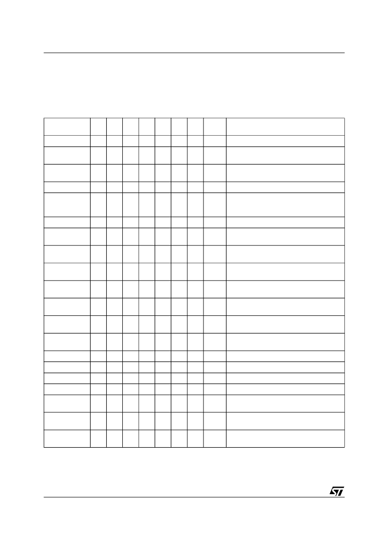
PSD REGISTER DESCRIPTION AND ADDRESS OFFSETS
Table 6 shows the offset addresses to the PSD
registers relative to the CSIOP base address. The
CSIOP space is the 256 bytes of address that is al-
located by the user to the internal PSD registers.
Table 6 provides brief descriptions of the registers
in CSIOP space. The following sections give a
more detailed description.
Table 6. Register Address Offset
Note: 1. Other registers that are not part of the I/O ports.
Register Name
Port
A
Port
B
Port
C
Port
D
Port
E
Port
F
Port
G
Other
1
Description
Data In
00
01
10
11
30
40
41
Reads Port pin as input, MCU I/O input mode
Control
32
42
43
Selects mode between MCU I/O or Address
Out
Data Out
04
05
14
15
34
44
45
Stores data for output to Port pins, MCU I/O
output mode
Direction
06
07
16
17
36
46
47
Configures Port pin as input or output
Drive Select
08
09
18
19
38
48
49
Configures Port pins as either CMOS or
Open Drain on some pins, while selecting
high slew rate on other pins.
Input Macrocell
0A
0B
1A
Reads Input Macrocells
Enable Out
0C
0D
1C
4C
Reads the status of the output enable to the
I/O Port driver
Output
Macrocells A
20
Read – reads output of Macrocells A
Write – loads Macrocell Flip-flops
Output
Macrocells B
21
Read – reads output of Macrocells B
Write – loads Macrocell Flip-flops
Mask
Macrocells A
22
Blocks writing to the Output Macrocells A
Mask
Macrocells B
23
Blocks writing to the Output Macrocells B
Flash Memory
Protection
C0
Read only – Primary Flash Sector Protection
Flash Boot
Protection
C2
Read only – PSD Security and Secondary
Flash memory Sector Protection
JTAG Enable
C7
Enables JTAG Port
PMMR0
B0
Power Management Register 0
PMMR2
B4
Power Management Register 2
Page
E0
Page Register
VM
E2
Places PSD memory areas in Program and/
or Data space on an individual basis.
Memory_ID0
F0
Read only – SRAM and Primary memory
size
Memory_ID1
F1
Read only – Secondary memory type and
size
相关PDF资料 |
PDF描述 |
|---|---|
| PSD501B1 | Field Programmable Microcontroller Peripherals(可编程逻辑,16K位SRAM,40个可编程I/O,通用PLD有61个输入) |
| PSD511B1 | Field Programmable Microcontroller Peripherals(可编程逻辑,16K位SRAM,40个可编程I/O,通用PLD有61个输入) |
| PSD502B1 | Field Programmable Microcontroller Peripherals(可编程逻辑,16K位SRAM,40个可编程I/O,通用PLD有61个输入) |
| PSD503B1 | Field Programmable Microcontroller Peripherals(可编程逻辑,16K位SRAM,40个可编程I/O,通用PLD有61个输入) |
| PSD502B1-12U | 200V 100kRad Hi-Rel Single N-Channel TID Hardened MOSFET in a TO-204AE package; Similar to IRH7250 with optional Total Dose Rating of 1000kRads |
相关代理商/技术参数 |
参数描述 |
|---|---|
| PSD4235G2-70U | 功能描述:SPLD - 简单可编程逻辑器件 5.0V 4M 70ns RoHS:否 制造商:Texas Instruments 逻辑系列:TICPAL22V10Z 大电池数量:10 最大工作频率:66 MHz 延迟时间:25 ns 工作电源电压:4.75 V to 5.25 V 电源电流:100 uA 最大工作温度:+ 75 C 最小工作温度:0 C 安装风格:Through Hole 封装 / 箱体:DIP-24 |
| PSD4235G2-90U | 功能描述:CPLD - 复杂可编程逻辑器件 5.0V 4M 90ns RoHS:否 制造商:Lattice 系列: 存储类型:EEPROM 大电池数量:128 最大工作频率:333 MHz 延迟时间:2.7 ns 可编程输入/输出端数量:64 工作电源电压:3.3 V 最大工作温度:+ 90 C 最小工作温度:0 C 封装 / 箱体:TQFP-100 |
| PSD4235G2-90UI | 功能描述:CPLD - 复杂可编程逻辑器件 5.0V 4M 90ns RoHS:否 制造商:Lattice 系列: 存储类型:EEPROM 大电池数量:128 最大工作频率:333 MHz 延迟时间:2.7 ns 可编程输入/输出端数量:64 工作电源电压:3.3 V 最大工作温度:+ 90 C 最小工作温度:0 C 封装 / 箱体:TQFP-100 |
| PSD4235G2V-12UI | 功能描述:CPLD - 复杂可编程逻辑器件 3.3V 4M 120ns RoHS:否 制造商:Lattice 系列: 存储类型:EEPROM 大电池数量:128 最大工作频率:333 MHz 延迟时间:2.7 ns 可编程输入/输出端数量:64 工作电源电压:3.3 V 最大工作温度:+ 90 C 最小工作温度:0 C 封装 / 箱体:TQFP-100 |
| PSD4235G2V-90U | 功能描述:CPLD - 复杂可编程逻辑器件 3.3V 4M 90ns RoHS:否 制造商:Lattice 系列: 存储类型:EEPROM 大电池数量:128 最大工作频率:333 MHz 延迟时间:2.7 ns 可编程输入/输出端数量:64 工作电源电压:3.3 V 最大工作温度:+ 90 C 最小工作温度:0 C 封装 / 箱体:TQFP-100 |
发布紧急采购,3分钟左右您将得到回复。