- 您现在的位置:买卖IC网 > PDF目录368262 > PSD835G2V-A-15B81I (意法半导体) Configurable Memory System on a Chip for 8-Bit Microcontrollers PDF资料下载
参数资料
| 型号: | PSD835G2V-A-15B81I |
| 厂商: | 意法半导体 |
| 英文描述: | Configurable Memory System on a Chip for 8-Bit Microcontrollers |
| 中文描述: | 在8片位微控制器可配置存储系统 |
| 文件页数: | 9/110页 |
| 文件大小: | 570K |
| 代理商: | PSD835G2V-A-15B81I |
第1页第2页第3页第4页第5页第6页第7页第8页当前第9页第10页第11页第12页第13页第14页第15页第16页第17页第18页第19页第20页第21页第22页第23页第24页第25页第26页第27页第28页第29页第30页第31页第32页第33页第34页第35页第36页第37页第38页第39页第40页第41页第42页第43页第44页第45页第46页第47页第48页第49页第50页第51页第52页第53页第54页第55页第56页第57页第58页第59页第60页第61页第62页第63页第64页第65页第66页第67页第68页第69页第70页第71页第72页第73页第74页第75页第76页第77页第78页第79页第80页第81页第82页第83页第84页第85页第86页第87页第88页第89页第90页第91页第92页第93页第94页第95页第96页第97页第98页第99页第100页第101页第102页第103页第104页第105页第106页第107页第108页第109页第110页
PSD8XX Family
PSD835G2
8
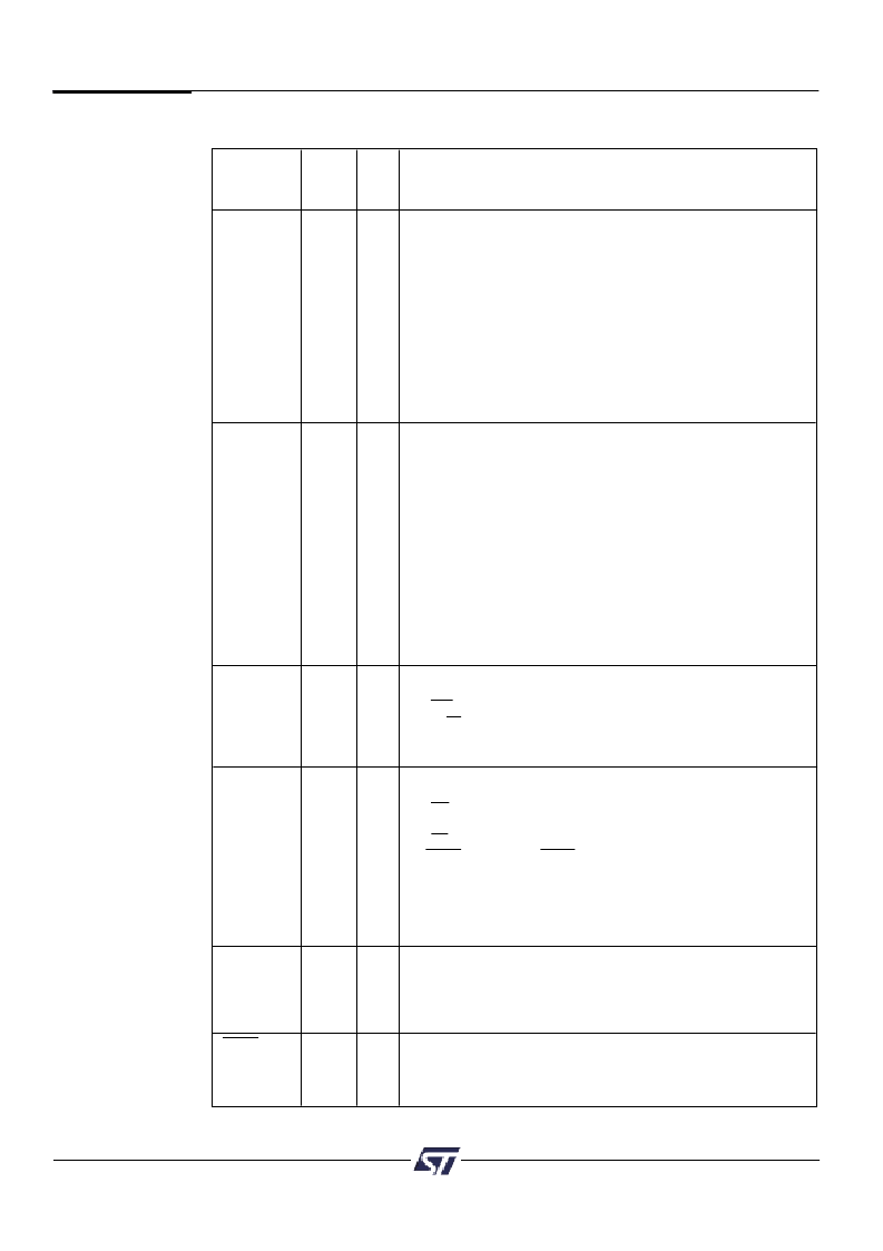
The following table describes the pin names and pin functions of the PSD835G2. Pins that
have multiple names and/or functions are defined using PSDsoft.
6.0
Table 5.
PSD835G2
Pin
Descriptions
Pin*
(TQFP
Pkg.)
Pin Name
Type
Description
ADIO0-7
3-7
10-12
I/O
This is the lower Address/Data port. Connect your MCU
address or address/data bus according to the following rules:
1. If your MCU has a multiplexed address/data bus where the
data is multiplexed with the lower address bits, connect
AD[0:7] to this port.
2. If your MCU does not have a multiplexed address/data bus,
connect A[0:7] to this port.
3. If you are using an 80C51XA in burst mode, connect
A4/D0 through A11/D7 to this port.
ALE or AS latches the address. The PSD drives data out only
if the read signal is active and one of the PSD functional blocks
was selected. The addresses on this port are passed to the
PLDs.
ADIO8-15
13-20
I/O
This is the upper Address/Data port. Connect your MCU
address or address/data bus according to the following rules:
1. If your MCU has a multiplexed address/data bus where the
data is multiplexed with the lower address bits, connect
A[8:15] to this port.
2. If your MCU does not have a multiplexed address/data bus,
connect A[8:15] to this port.
3. If you are using an 80C251 in page mode, connect AD[8:15]
to this port
4. If you are using an 80C51XA in burst mode, connect
A[12:19] to this port.
ALE or AS latches the address. The PSD drives data out only
if the read signal is active and one of the PSD functional
blocks was selected. The addresses on this port are passed
to the PLDs.
CNTL0
59
I
The following control signals can be connected to this port,
based on your MCU:
1. WR — active-low write input.
2. R_W — active-high read/active low write input.
This pin is connected to the PLDs. Therefore, these signals can
be used in decode and other logic equations.
CNTL1
60
I
The following control signals can be connected to this port,
based on your MCU:
1. RD — active-low read input.
2. E — E clock input.
3. DS — active-low data strobe input.
4. PSEN — connect PSEN to this port when it is being used as
an active-low read signal. For example, when the 80C251
outputs more than 16 address bits, PSEN is actually the read
signal.
This pin is connected to the PLDs. Therefore, these signals can
be used in decode and other logic equations.
CNTL2
40
I
This pin can be used to input the PSEN (Program Select
Enable) signal from any MCU that uses this signal for code
exclusively. If your MCU does not output a Program Select
Enable signal, this port can be used as a generic input. This
port is connected to the PLD as input.
Active low input. Resets I/O Ports, PLD Micro
Cells, some of
the configuration registers and JTAG registers. Must be active
at power up. Reset also aborts the Flash programming/erase
cycle that is in progress.
Reset
39
I
相关PDF资料 |
PDF描述 |
|---|---|
| PSD835G2V-A-15J | Configurable Memory System on a Chip for 8-Bit Microcontrollers |
| PSD835G2V-A-15JI | Configurable Memory System on a Chip for 8-Bit Microcontrollers |
| PSD835G2V-A-15M | Configurable Memory System on a Chip for 8-Bit Microcontrollers |
| PSD835G2V-A-15MI | Configurable Memory System on a Chip for 8-Bit Microcontrollers |
| PSD835G2V-A-15U | Configurable Memory System on a Chip for 8-Bit Microcontrollers |
相关代理商/技术参数 |
参数描述 |
|---|---|
| PSD853F2-70J | 功能描述:SPLD - 简单可编程逻辑器件 5.0V 1M 70ns RoHS:否 制造商:Texas Instruments 逻辑系列:TICPAL22V10Z 大电池数量:10 最大工作频率:66 MHz 延迟时间:25 ns 工作电源电压:4.75 V to 5.25 V 电源电流:100 uA 最大工作温度:+ 75 C 最小工作温度:0 C 安装风格:Through Hole 封装 / 箱体:DIP-24 |
| PSD853F2-70M | 功能描述:CPLD - 复杂可编程逻辑器件 5.0V 1M 70ns RoHS:否 制造商:Lattice 系列: 存储类型:EEPROM 大电池数量:128 最大工作频率:333 MHz 延迟时间:2.7 ns 可编程输入/输出端数量:64 工作电源电压:3.3 V 最大工作温度:+ 90 C 最小工作温度:0 C 封装 / 箱体:TQFP-100 |
| PSD853F2-90J | 功能描述:CPLD - 复杂可编程逻辑器件 5.0V 1M 90ns RoHS:否 制造商:Lattice 系列: 存储类型:EEPROM 大电池数量:128 最大工作频率:333 MHz 延迟时间:2.7 ns 可编程输入/输出端数量:64 工作电源电压:3.3 V 最大工作温度:+ 90 C 最小工作温度:0 C 封装 / 箱体:TQFP-100 |
| PSD853F2-90JI | 功能描述:CPLD - 复杂可编程逻辑器件 5.0V 1M 90ns RoHS:否 制造商:Lattice 系列: 存储类型:EEPROM 大电池数量:128 最大工作频率:333 MHz 延迟时间:2.7 ns 可编程输入/输出端数量:64 工作电源电压:3.3 V 最大工作温度:+ 90 C 最小工作温度:0 C 封装 / 箱体:TQFP-100 |
| PSD853F2-90M | 功能描述:CPLD - 复杂可编程逻辑器件 5.0V 1M 90ns RoHS:否 制造商:Lattice 系列: 存储类型:EEPROM 大电池数量:128 最大工作频率:333 MHz 延迟时间:2.7 ns 可编程输入/输出端数量:64 工作电源电压:3.3 V 最大工作温度:+ 90 C 最小工作温度:0 C 封装 / 箱体:TQFP-100 |
发布紧急采购,3分钟左右您将得到回复。