- 您现在的位置:买卖IC网 > PDF目录69251 > PTB48510BAH (TEXAS INSTRUMENTS INC) 2-OUTPUT 72 W DC-DC REG PWR SUPPLY MODULE PDF资料下载
参数资料
| 型号: | PTB48510BAH |
| 厂商: | TEXAS INSTRUMENTS INC |
| 元件分类: | 电源模块 |
| 英文描述: | 2-OUTPUT 72 W DC-DC REG PWR SUPPLY MODULE |
| 封装: | DIP-8 |
| 文件页数: | 12/17页 |
| 文件大小: | 544K |
| 代理商: | PTB48510BAH |
www.ti.com
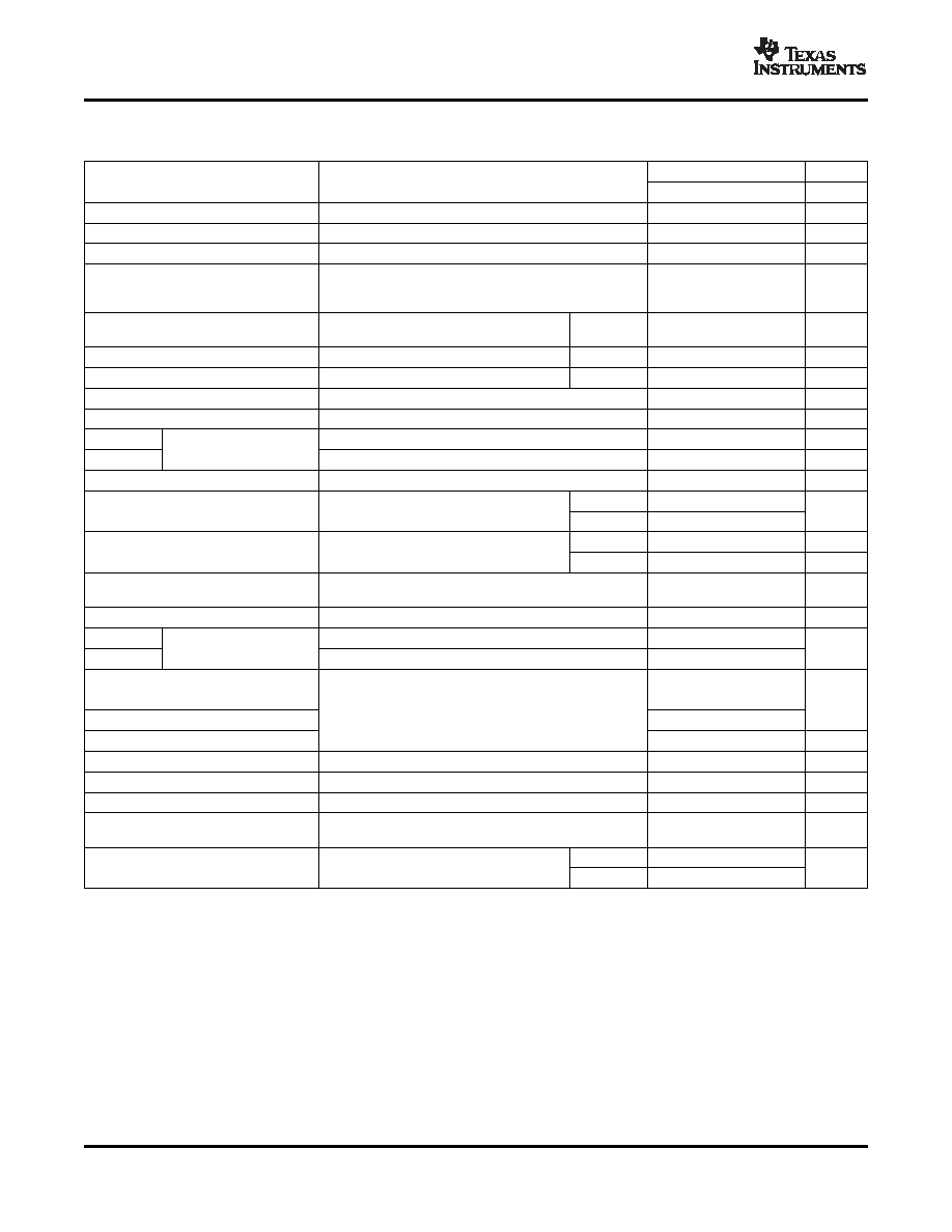
ELECTRICAL CHARACTERISTICS
SLTS219F – FEBRUARY 2004 – REVISED MARCH 2007
(Unless otherwise stated, TA = 25°C, VI = 48 V, CI = 0 F, CO = 0 F, IO1 = IO2 = 3.25 A maximum)
PTB4851xB
PARAMETER
TEST CONDITIONS
MIN
TYP
MAX
UNIT
PO
Output Power
Total output power from VO1or VO1
0
72(1)
W
IO1 or IO2
Output Current
Over VI range, IO1 ≤ 0.1 A or IO2 ≤ 0.1 A ≤ 0.1 A
0
3(2)
A
IO1 - IO2
Output Load Imbalance
IO1 ≥ 0.1 A, IO2 ≥ 0.1 A
0
1(3)
A
Includes set point, line, load, IO1 ≤ 0.1 A or IO2 ≤ 0.1 A ≤
VO1 or VO2
Output Voltage
0.1 A
11.6(2)
12 12.4(2)
V
–40
°C ≤ T
A ≤ 85°C
–40
°C ≤ T
A ≤ 85°C, IO1 ≤ 0.1 A or IO2 ≤ 0.1
VO1 or VO2
±1
ΔRegtemp
Temperature Variation
%VO
A
ΔRegline
Line Regulation
Over VI range, balanced load
VO1 or VO2
±0.05
±0.5
%VO
ΔRegload
Load Regulation
Over IO1 or IO2 range, balanced load
VO1 or VO2
±0.1
±1
%VO
η
Efficiency
89%
Vr
VO Ripple (pk-pk)
20 MHz bandwidth, CO = 10 F tantalum capacitor
20
80(4)
mVpp
ttr
0.1 A/
s load step, 50% to 75% I
O1 or IO2 maximum
30
s
Transient Response
ΔVtr
VO1 or VO2 overshoot/undershoot
±1
%VO
IOtrip
Overcurrent Threshold
VI = 36 V, reset followed by auto-recovery
3.3
3.8
5
A
PTB48510A
NA
VO1(trip),
Overvoltage Threshold
Outputs latched off (5)
V
VO2(trip)
PTB48511A
14
15.8
17
IO1(pk) IO2(pk)
6
A
Short Circuit Current
Continuous overcurrent trip, IO1 = IO2
Duty
10%
VO1(adj),
Output Voltage Adjust
VO1 and VO2 adjust simultaneously
6.5
13.4
V
VO2(adj)
Range
f S
Switching Frequency
Over VI and IO ranges
440
480(6)
500
kHz
VI on
VI increasing
33
Under-Voltage Lockout
V
VI off
VI decreasing
32
On/Off Enable (pin 3)
Referenced to VI (pin 4)
VIH
High-level input voltage
3.6
75(7)
V
VIL
Low-level input voltage
–0.2
0.8
IIL
Low-level input current
–1
mA
II standby
Standby Input Current
Pin 3 open circuit
2
mA
tON
Start-up Time
IO1 ≤ 1 A or IO2 ≤ 1 A, VO1 or VO2 rising 0 to 0.95 (typ)
6
12
18
ms
CI
Internal Input Capacitance
3
F
External Output
3000(8
CO
Capacitance from either output to COM (pin 6)
0
F
Capacitance
)
PTB48510B
2.8
Per Telcordia SR-332 50% stress,
MTBF
Reliability
106 Hrs
TA = 40°C, ground benign
PTB48511B
2.5
(1)
See Safe Operating Area curves or contact the factory for the appropriate derating.
(2)
Under balanced load conditions, load current flowing out of VO1 is balanced to within ±0.1 A of that flowing into VO2.
(3)
A load imbalance is the difference in current flowing from VO1 to VO2. The module can operate with a higher imbalance but with reduced
specifications.
(4)
Output voltage ripple is measured with a 10
F tantalum capacitor connected from V
O1 (pin 5) or VO2 (pin 8), to COM (pin 6).
(5)
If the overvoltage threshold is exceeded by either regulated output the module will shut down, turning both outputs off. This is a latched
condition, which can only by reset by removing and then re-applying the module's input power.
(6)
This is the free-running frequency. The module can be made to synchronize with the PTB48500 when both modules are used together
in a system.
(7)
The On/Off Enable (pin 3) has an internal pull-up and may be controlled with an open-collector (or open-drain) transistor. The input is
diode protected and may be connected to VI. The open-circuit voltage is 5 V maximum. If it is left open circuit the converter operates
when input power is applied.
(8)
Electrolytic capacitors with very low equivalent series resistance (ESR) may induce instability when used on the output. Consult the
factory before using capacitors with organic, or polymer-aluminum type electrolytes.
4
Copyright 2004–2007, Texas Instruments Incorporated
相关PDF资料 |
PDF描述 |
|---|---|
| PTB48510CAS | 2-OUTPUT 66 W DC-DC REG PWR SUPPLY MODULE |
| PTB48520WAH | 1-OUTPUT DC-DC REG PWR SUPPLY MODULE |
| PTB48520WAS | 1-OUTPUT DC-DC REG PWR SUPPLY MODULE |
| PTB48520WAZ | 1-OUTPUT DC-DC REG PWR SUPPLY MODULE |
| PTB48560AAS | 1-OUTPUT 30 W DC-DC REG PWR SUPPLY MODULE |
相关代理商/技术参数 |
参数描述 |
|---|---|
| PTB48510BAS | 功能描述:DC/DC转换器 72W+/-12V Dual Comp Outp DC/DC Converter RoHS:否 制造商:Murata 产品: 输出功率: 输入电压范围:3.6 V to 5.5 V 输入电压(标称): 输出端数量:1 输出电压(通道 1):3.3 V 输出电流(通道 1):600 mA 输出电压(通道 2): 输出电流(通道 2): 安装风格:SMD/SMT 封装 / 箱体尺寸: |
| PTB48510BAZ | 功能描述:DC/DC转换器 72W+/-12V Dual Comp Outp DC/DC Converter RoHS:否 制造商:Murata 产品: 输出功率: 输入电压范围:3.6 V to 5.5 V 输入电压(标称): 输出端数量:1 输出电压(通道 1):3.3 V 输出电流(通道 1):600 mA 输出电压(通道 2): 输出电流(通道 2): 安装风格:SMD/SMT 封装 / 箱体尺寸: |
| PTB48510C | 制造商:TI 制造商全称:Texas Instruments 功能描述:Dual Complementary-Output DC/DC Converter for DSL |
| PTB48510CAH | 功能描述:DC/DC转换器 66W+/- 5V Dual Comp Outp DC/DC Converter RoHS:否 制造商:Murata 产品: 输出功率: 输入电压范围:3.6 V to 5.5 V 输入电压(标称): 输出端数量:1 输出电压(通道 1):3.3 V 输出电流(通道 1):600 mA 输出电压(通道 2): 输出电流(通道 2): 安装风格:SMD/SMT 封装 / 箱体尺寸: |
| PTB48510CAS | 功能描述:DC/DC转换器 66W+/- 5V Dual Comp Outp DC/DC Converter RoHS:否 制造商:Murata 产品: 输出功率: 输入电压范围:3.6 V to 5.5 V 输入电压(标称): 输出端数量:1 输出电压(通道 1):3.3 V 输出电流(通道 1):600 mA 输出电压(通道 2): 输出电流(通道 2): 安装风格:SMD/SMT 封装 / 箱体尺寸: |
发布紧急采购,3分钟左右您将得到回复。