- 您现在的位置:买卖IC网 > PDF目录98066 > PTR08100WVD (TEXAS INSTRUMENTS INC) 10 A SWITCHING REGULATOR, 300 kHz SWITCHING FREQ-MAX, PSIP5 PDF资料下载
参数资料
| 型号: | PTR08100WVD |
| 厂商: | TEXAS INSTRUMENTS INC |
| 元件分类: | 稳压器 |
| 英文描述: | 10 A SWITCHING REGULATOR, 300 kHz SWITCHING FREQ-MAX, PSIP5 |
| 封装: | PLASTIC, DSS-5 |
| 文件页数: | 10/15页 |
| 文件大小: | 334K |
| 代理商: | PTR08100WVD |
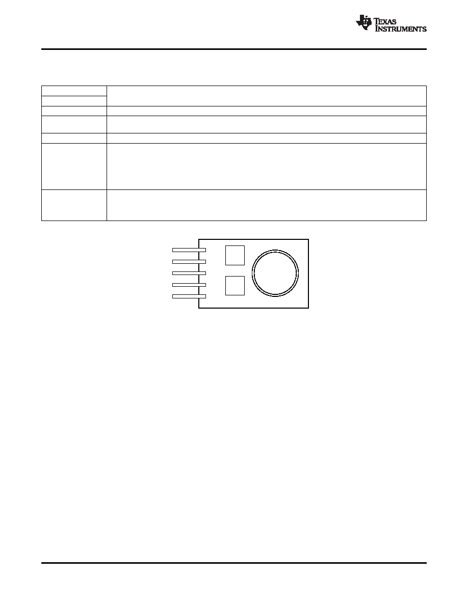
PIN ASSIGNMENT
1
2
3
4
5
SLTS284E – AUGUST 2007 – REVISED APRIL 2009 ....................................................................................................................................................... www.ti.com
TERMINAL FUNCTIONS
TERMINAL
DESCRIPTION
NAME
NO.
VI
2
The positive input voltage power node to the module, which is referenced to common GND.
This is the common ground connection for the VI and VO power connections. It is also the 0 VDC reference for the
GND
3
Inhibit and VO Adjust control inputs.
VO
4
The regulated positive power output with respect to the GND node.
A 1% resistor must be connected between this pin and GND (pin 3) to set the output voltage of the module higher
than 0.6 V. If left open-circuit, the output voltage defaults to this value. The temperature stability of the resistor
should be 100 ppm/°C (or better). The set-point range is from 0.6 V to 5.5 V. For information on output voltage
VOAdjust
5
adjustment see the related application section.
TheVOAdjust pin must never be connected directly to GND. The minimum resistance between VOAdjust and
GND is limited to 240
.
The Inhibit pin is an open-collector/drain-negative logic input that is referenced to GND. Applying a low-level ground
signal to this input disables the module's output. When the Inhibit control is active, the input current drawn by the
Inhibit
1
regulator is significantly reduced. If the Inhibit pin is left open-circuit, the module will produce an output voltage
whenever a valid input source is applied.
TOP VIEW
4
Copyright 2007–2009, Texas Instruments Incorporated
Product Folder Link(s): PTR08100W
相关PDF资料 |
PDF描述 |
|---|---|
| PTV03020WAH | 1-OUTPUT DC-DC REG PWR SUPPLY MODULE |
| PTV05010WAH | 1-OUTPUT DC-DC REG PWR SUPPLY MODULE |
| PTV08T250WAH | 1-OUTPUT DC-DC REG PWR SUPPLY MODULE |
| PTV08T250WAD | 1-OUTPUT DC-DC REG PWR SUPPLY MODULE |
| PTV12010WAD | 1-OUTPUT DC-DC REG PWR SUPPLY MODULE |
相关代理商/技术参数 |
参数描述 |
|---|---|
| PTR1 | 制造商:Panduit Corp 功能描述: |
| PTR-1 | 制造商:Greenlee Textron Inc 功能描述:REPLACEMENT KIT TIP NAILEATER-1" |
| PTR12 | 制造商:Pentair Technical Products / Hoffman 功能描述:Transformer Rails (2) , fits 1200mm wide, Steel |
| P-TR12 | 制造商:Pentair Technical Products / Hoffman 功能描述:Transformer Rails (2) |
| PTR156F22-2-D | 制造商:ITW Pancon 功能描述: |
发布紧急采购,3分钟左右您将得到回复。