- 您现在的位置:买卖IC网 > PDF目录299793 > PUMA68F4001MB-15 128K X 32 FLASH 5V PROM MODULE, 150 ns, PQMA68 PDF资料下载
参数资料
| 型号: | PUMA68F4001MB-15 |
| 元件分类: | PROM |
| 英文描述: | 128K X 32 FLASH 5V PROM MODULE, 150 ns, PQMA68 |
| 封装: | PLASTIC, LCC-68 |
| 文件页数: | 11/12页 |
| 文件大小: | 495K |
| 代理商: | PUMA68F4001MB-15 |
PUMA 68F4001-15/17/20
ISSUE 4.1 : AUGUST 1997
8
Hardware Data Protection
Both hardware and software protection is provided as described below.
Four types of hardware protection give high security against accidental writes:
If V
cc - 3.8V, Write is inhibited.
OE low, CS or WE high inhibits inadvertant Write Cycles during power-on and power-off. Write Cycle timing
specifications must be observed concurrently.
Pulses are less than 20ns on WE do not initiate a Write Cycle.
Software controlled data protection, once enabled by the user, means that a software algorithm must be used
before any write can be performed. To enable this feature the algorithm opposite is followed, and must be
reused for each subsequent write operation. Once set the data protection remains operational until it is
disabled by using the second algorithm overleaf: power transitions will not reset this feature.
Notes:
(1) Data Format I/O7-I/O0 (Hex);
Once initiated, this sequence of write opera-
tions should not be interrupted.
(2) Enable Write Protect state will be initiated at end of
write even if no other data is loaded.
(3) Disable Write Protect state will be initiated at end of
write period even if no other data is loaded.
(4) 128 bytes of data must be loaded.
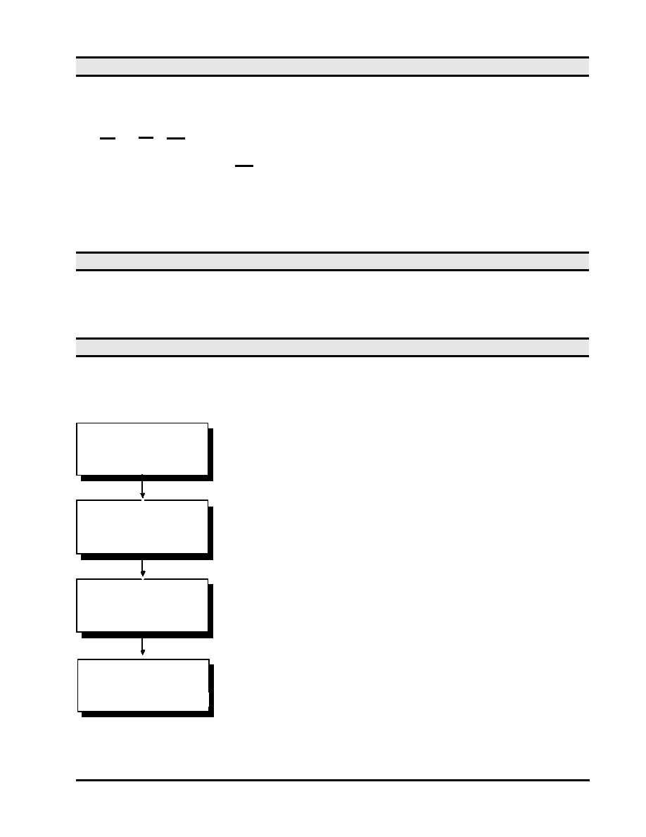
LOAD DATA A0
TO
ADDRESS 5555
LOAD DATA 55
TO
ADDRESS 2AAA
LOAD DATA AA
TO
ADDRESS 5555
LOAD DATA
TO
SECTOR (128 BYTES)
(4)
WRITES
ENABLED (2)
ENTER DATA
PROTECT
STATE
Software Algorithms
Selecting the software data protection mode requires the host system to precede datawrite operations by a series
of three write operations to three specfic addresses. The three byte sequence opens the page write window
enabling the host to write 128 bytes of data. Once the page load cycle has been completed, the device will
automatically be returned to the data protected state
Software Data Protection Algorithm (1)
Regardless of whether the device has been protected or not, once the software data protected algorithm is used
and the data is written, the PUMA 68F4001 will automatically disable further writes unless another command is
issued to cancel it. If no further commands are issued the PUMA 68F4001 will be write protected during power-
down and any subsequent power-up.
相关PDF资料 |
PDF描述 |
|---|---|
| PUMA68S16000XBL-012 | 512K X 32 MULTI DEVICE SRAM MODULE, 12 ns, PQCC68 |
| PUMA68SV16000B-020 | 512K X 32 MULTI DEVICE SRAM MODULE, 20 ns, PQMA68 |
| PUMA68SV16000B-35 | 512K X 32 MULTI DEVICE SRAM MODULE, 35 ns, PQMA68 |
| PUMA77FV16006AM-90E | 256 CABGA, IND TEMP(FPGA) |
| PUMA77FV16006AMB-120 | EEPROM |
相关代理商/技术参数 |
参数描述 |
|---|---|
| PUMA68F4001MB-17 | 制造商:未知厂家 制造商全称:未知厂家 功能描述:x32 Flash EEPROM Module |
| PUMA68F4001MB-20 | 制造商:未知厂家 制造商全称:未知厂家 功能描述:x32 Flash EEPROM Module |
| PUMA68F4003-12 | 制造商:未知厂家 制造商全称:未知厂家 功能描述:x32 Flash EEPROM Module |
| PUMA68F4003-15 | 制造商:未知厂家 制造商全称:未知厂家 功能描述:x32 Flash EEPROM Module |
| PUMA68F4003-20 | 制造商:未知厂家 制造商全称:未知厂家 功能描述:x32 Flash EEPROM Module |
发布紧急采购,3分钟左右您将得到回复。