- 您现在的位置:买卖IC网 > PDF目录69294 > PWR-82333-120L (DATA DEVICE CORP) BRUSHLESS DC MOTOR CONTROLLER, 50 A, DMA26 PDF资料下载
参数资料
| 型号: | PWR-82333-120L |
| 厂商: | DATA DEVICE CORP |
| 元件分类: | 运动控制电子 |
| 英文描述: | BRUSHLESS DC MOTOR CONTROLLER, 50 A, DMA26 |
| 封装: | 3 X 2.100 INCH, 0.390 INCH HEIGHT, PACKAGE-26 |
| 文件页数: | 11/17页 |
| 文件大小: | 631K |
| 代理商: | PWR-82333-120L |
3
Data Device Corporation
www.ddc-web.com
PWR-82331 and PWR-82333
P-02/05-0
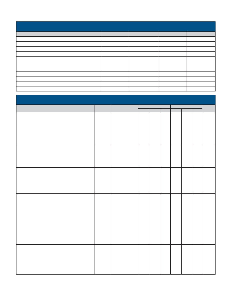
TABLE 1. PWR-82331 AND PWR-82333 ABSOLUTE MAXIMUM RATINGS
(TC = +25°C UNLESS OTHERWISE SPECIFIED)
PARAMETER
SYMBOL
PWR-82331
PWR-82333
UNITS
SUPPLY VOLTAGE
VCC
200
500
V
BIAS VOLTAGE
VB
50
V
LOGIC POWER-IN VOLTAGE
VLPI
18
V
INPUT LOGIC VOLTAGE
VU, VL, VSd
VLPI + 0.5
V
OUTPUT CURRENT
Continuous
Pulsed
IO
IOP
30
50
30
50
A
OPERATING FREQUENCY
fo
50
25
kHz
CASE OPERATING TEMPERATURE
TC
-55 to +125
°C
GND - VSS DIFFERENTIAL VOLTAGE
CASE STORAGE TEMPERATURE RANGE
TCS
± 3
-55 to +150
± 3
-55 to +150
Vdc-peak
°C
TABLE 2. PWR-82331 AND PWR-82333 SPECIFICATIONS
(TC = +25°C UNLESS OTHERWISE SPECIFIED)
PARAMETER
SYMBOL
TEST
CONDITIONS
PWR-82331
UNITS
PWR-82333
MIN
TYP
MAX
MIN
MAX
TYP
OUTPUT
Output Current Continuous (see FIG.’s 15 & 19)
Supply Voltage
Output On-Resistance (each FET)(see FIG. 14A)
Output Voltage drop (each IGBT) (see FIG. 14B)
Instant Forward Voltage (flyback diode) (see FIG.’s 13A/B
Reverse Recovery Time (flyback diode)
Reverse Leakage Current at TC = +25°C
Reverse Leakage Current at TC = +125°C
IO
VCC
RON
VCE(SAT)
VF
trr
Ir
see note 1
IO=30 A
IOP=30 A, see note 2
If=1 A, Ir=1 A
see note 3
28
30
140
0.1
1.15
50
10
1
A
V
ohm
V
nsec
A
mA
30
350
3.8
1.70
50
10
1
270
BIAS SUPPLY
Input Bias Voltage (TC= -55°C to +125°C)
Quiescent Bias Current (see note 4)(see FIG. 16)
Bias Current (TC= -55°C to +125°C)(see FIG.’s 17 & 18)
In-rush Current (TC= -55°C to +125°C)
Logic power Input Current
Vb
Ibq
Ib
Iir
ILPI
Vb = 28 V
Vb=28 V, see note 5
Vb = 28 V
see note 6
14
35
32
50
65
1.4
2
14
35
V
mA
A
mA
50
65
1.4
2
32
INPUT SIGNALS (SEE FIG. 7)
Positive Trigger Threshold Voltage
Negative Trigger Threshold Voltage
Hysteresis Voltage
Positive Trigger Threshold Voltage
Negative Trigger Threshold Voltage
Hysteresis Voltage
VP
VN
VH
VP
VN
VH
Pin Connections
Pin 15 &16 connect.
Pin 15 &16 connect
See note 6
2.1
1.6
0.9
0.3
12.9
10.8
4.3
3.6
2.1
1.6
0.9
0.3
V
12.9
10.8
4.3
3.6
SWITCHING CHARACTERISTICS (SEE FIG. 2)
Upper Drive:
Turn-on propagation delay
Turn-off propagation delay
Shut-down propagation delay
Turn-on Rise Time
Turn-off Fall Time
Lower Drive:
Turn-on propagation delay
Turn-off propagation delay
Shut-down propagation delay
Turn-on Rise Time
Turn-off Fall Time
td(on)
td(off)
tSd
tr
tf
td(on)
td(off)
tSd
tr
tf
Test 1 Conditions
Pin 15 &16 connect.
+15 V Logic
Io=30 A peak
PWR-82331,
VCC = 140 V
PWR-82333,
VCC = 270 V
840
1020
800
125
850
1000
800
125
nsec
810
860
810
100
150
800
870
770
100
150
SWITCHING CHARACTERISTICS (SEE FIG. 2)
Upper Drive:
Turn-on propagation delay
Turn-off propagation delay
Shut-down propagation delay
Turn-on Rise Time
Turn-off Fall Time
td(on)
td(off)
tSd
tr
tf
Test 2 Conditions
see note 6
+5 V, Io=30 A peak
PWR-82331,
Vcc = 140 V
PWR-82333,
VCC = 270 V
1090
1315
1100
125
nsec
1050
1150
850
100
150
相关PDF资料 |
PDF描述 |
|---|---|
| PWR-82333-210 | BRUSHLESS DC MOTOR CONTROLLER, 50 A, DMA26 |
| PWR-82333-410Q | BRUSHLESS DC MOTOR CONTROLLER, 50 A, DMA26 |
| PWR-82333-500L | BRUSHLESS DC MOTOR CONTROLLER, 50 A, DMA26 |
| PWR-82331-400S | BRUSHLESS DC MOTOR CONTROLLER, 50 A, DMA26 |
| PWR-82331-810L | BRUSHLESS DC MOTOR CONTROLLER, 50 A, DMA26 |
相关代理商/技术参数 |
参数描述 |
|---|---|
| PWR-82333-200 | 制造商:未知厂家 制造商全称:未知厂家 功能描述:DC Motor Controller/Driver |
| PWR-82333-300 | 制造商:未知厂家 制造商全称:未知厂家 功能描述:DC Motor Controller/Driver |
| PWR-82340 | 制造商:未知厂家 制造商全称:未知厂家 功能描述:Drives (Power Amplifiers)|3-Phase Bridge Drive. Flat Pack Hybrid with Formed Leads |
| PWR-82340-100 | 制造商:未知厂家 制造商全称:未知厂家 功能描述:DC Motor Controller/Driver |
| PWR-82340-110 | 制造商:未知厂家 制造商全称:未知厂家 功能描述:DC Motor Controller/Driver |
发布紧急采购,3分钟左右您将得到回复。