- 您现在的位置:买卖IC网 > PDF目录20638 > PX3511BDAG-R3 (Intersil)IC DRVR SYNC BUCK HF 8-SOIC PDF资料下载
参数资料
| 型号: | PX3511BDAG-R3 |
| 厂商: | Intersil |
| 文件页数: | 4/10页 |
| 文件大小: | 0K |
| 描述: | IC DRVR SYNC BUCK HF 8-SOIC |
| 标准包装: | 2,500 |
| 配置: | 高端和低端,同步 |
| 输入类型: | PWM |
| 延迟时间: | 10ns |
| 电流 - 峰: | 1.25A |
| 配置数: | 1 |
| 输出数: | 2 |
| 高端电压 - 最大(自引导启动): | 36V |
| 电源电压: | 10.8 V ~ 13.2 V |
| 工作温度: | 0°C ~ 85°C |
| 安装类型: | 表面贴装 |
| 封装/外壳: | 8-SOIC(0.154",3.90mm 宽) |
| 供应商设备封装: | 8-SOIC |
| 包装: | 带卷 (TR) |
�� �
�
�PX3511A,� PX3511B�
�Absolute� Maximum� Ratings�
�Thermal� Information�
�Supply� Voltage� (VCC)� .� .� .� .� .� .� .� .� .� .� .� .� .� .� .� .� .� .� .� .� .� .� .� .� .� .� .� .� .� .� .� .� .15V�
�Thermal� Resistance�
�θ� JA� (°C/W)�
�θ� JC� (°C/W)�
�Supply� Voltage� (PVCC)� .� .� .� .� .� .� .� .� .� .� .� .� .� .� .� .� .� .� .� .� .� .� .� .� .� VCC� +� 0.3V�
�BOOT� Voltage� (V� BOOT� ).� .� .� .� .� .� .� .� .� .� .� .� .� .� .� .� .� .� .� .� .� .� .� .� .� .� .� .� .� .� .� .36V�
�Input� Voltage� (V� PWM� )� .� .� .� .� .� .� .� .� .� .� .� .� .� .� .� .� .� .� .� .� .� .� GND� -� 0.3V� to� 7V�
�UGATE.� .� .� .� .� .� .� .� .� .� .� .� .� .� .� .� .� .� .� V� PHASE� -� 0.3V� DC� to� V� BOOT� +� 0.3V�
�V� PHASE� -� 3.5V� (<100ns� Pulse� Width,� 2μJ)� to� V� BOOT� +� 0.3V�
�LGATE� .� .� .� .� .� .� .� .� .� .� .� .� .� .� .� .� .� .� .� .� .� .� GND� -� 0.3V� DC� to� V� PVCC� +� 0.3V�
�SOIC� Package� (Note� 1)� .� .� .� .� .� .� .� .� .� .� .� .� 100� N/A�
�DFN� Package� (Notes� 2,� 3)� .� .� .� .� .� .� .� .� .� .� 48� 7�
�Maximum� Junction� Temperature� (Plastic� Package)� .� .� .� .� .� .� .� +150°C�
�Maximum� Storage� Temperature� Range� .� .� .� .� .� .� .� .� .� .-65°C� to� +150°C�
�Maximum� Lead� Temperature� (Soldering� 10s)� .� .� .� .� .� .� .� .� .� .� .� .� +300°C�
�(SOIC� -� Lead� Tips� Only)�
�GND� -� 5V� (<100ns� Pulse� Width,� 2μJ)� to� V� PVCC� +� 0.3V�
�PHASE.� .� .� .� .� .� .� .� .� .� .� .� .� .� .� GND� -� 0.3V� DC� to� 15V� DC� (V� PVCC� =� 12V)�
�GND� -� 8V� (<400ns,� 20μJ)� to� 30V� (<200ns,� VBOOT-GND<36V)�
�ESD� Rating�
�Human� Body� Model� .� .� .� .� .� .� .� .� .� .� .� .� .� .� .� .� .� .� .� .� Class� I� JEDEC� STD�
�Recommended� Operating� Conditions�
�Ambient� Temperature� Range� .� .� .� .� .� .� .� .� .� .� .� .� .� .� .� .� .� .� .� .� 0°C� to� +85°C�
�Maximum� Operating� Junction� Temperature� .� .� .� .� .� .� .� .� .� .� .� .� .� +125°C�
�Supply� Voltage,� VCC� .� .� .� .� .� .� .� .� .� .� .� .� .� .� .� .� .� .� .� .� .� .� .� .� .� .� .� .� 12V� ±� 10%�
�Supply� Voltage� Range,� PVCC� .� .� .� .� .� .� .� .� .� .� .� .� .� .� .� .� 5V� to� 12V� ±� 10%�
�CAUTION:� Stresses� above� those� listed� in� “Absolute� Maximum� Ratings”� may� cause� permanent� damage� to� the� device.� This� is� a� stress� only� rating� and� operation� of� the�
�device� at� these� or� any� other� conditions� above� those� indicated� in� the� operational� sections� of� this� specification� is� not� implied.�
�NOTES:�
�1.� θ� JA� is� measured� with� the� component� mounted� on� a� high� effective� thermal� conductivity� test� board� in� free� air.�
�2.� θ� JA� is� measured� in� free� air� with� the� component� mounted� on� a� high� effective� thermal� conductivity� test� board� with� “direct� attach”� features.� See�
�Tech� Brief� TB379.�
�3.� For� θ� JC� ,� the� “case� temp”� location� is� the� center� of� the� exposed� metal� pad� on� the� package� underside.�
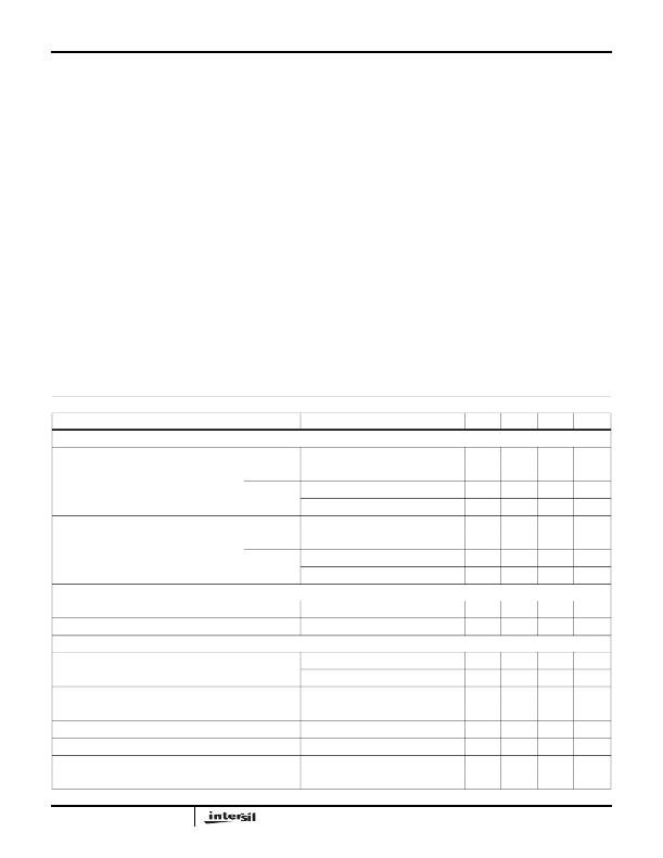
�Electrical� Specifications�
�Recommended� Operating� Conditions,� Unless� Otherwise� Noted.�
�PARAMETER�
�SYMBOL�
�TEST� CONDITIONS�
�MIN�
�TYP�
�MAX�
�UNITS�
�VCC� SUPPLY� CURRENT�
�Bias� Supply� Current�
�Gate� Drive� Bias� Current�
�I� VCC�
�I� VCC�
�I� PVCC�
�I� PVCC�
�(Note� 4)�
�PX3511A,� f� PWM� =� 300kHz,� V� VCC� =� 12V�
�PX3511B,� f� PWM� =� 300kHz,� V� VCC� =� 12V�
�PX3511A,� f� PWM� =� 1MHz,� V� VCC� =� 12V�
�PX3511B,� f� PWM� =� 1MHz,� V� VCC� =� 12V�
�PX3511A,� f� PWM� =� 300kHz,� V� PVCC� =� 12V�
�PX3511B,� f� PWM� =� 300kHz,� V� PVCC� =� 12V�
�PX3511A,� f� PWM� =� 1MHz,� V� PVCC� =� 12V�
�PX3511B,� f� PWM� =� 1MHz,� V� PVCC� =� 12V�
�-�
�-�
�-�
�-�
�-�
�-�
�-�
�-�
�8�
�4.5�
�10.5�
�5�
�4�
�7.5�
�5�
�8.5�
�-�
�-�
�-�
�-�
�-�
�-�
�-�
�-�
�mA�
�mA�
�mA�
�mA�
�mA�
�mA�
�mA�
�mA�
�POWER-ON� RESET� AND� ENABLE�
�VCC� Rising� Threshold�
�VCC� Falling� Threshold�
�9.35�
�7.35�
�9.8�
�7.6�
�10.0�
�8.0�
�V�
�V�
�PWM� INPUT� (See� Timing� Diagram� on� Page� 6)�
�Input� Current�
�PWM� Rising� Threshold� (Note� 4)�
�PWM� Falling� Threshold� (Note� 4)�
�Typical� Three-State� Shutdown� Window�
�Three-State� Lower� Gate� Falling� Threshold�
�Three-State� Lower� Gate� Rising� Threshold�
�Three-State� Upper� Gate� Rising� Threshold�
�I� PWM�
�V� PWM� =� 3.3V�
�V� PWM� =� 0V�
�VCC� =� 12V�
�VCC� =� 12V�
�VCC� =� 12V�
�VCC� =� 12V�
�VCC� =� 12V�
�VCC� =� 12V�
�-�
�-�
�-�
�-�
�1.23�
�-�
�-�
�-�
�505�
�-460�
�1.70�
�1.30�
�-�
�1.18�
�0.76�
�2.36�
�-�
�-�
�-�
�-�
�1.82�
�-�
�-�
�-�
�μA�
�μA�
�V�
�V�
�V�
�V�
�V�
�V�
�4�
�FN6462.0�
�February� 26,� 2007�
�相关PDF资料 |
PDF描述 |
|---|---|
| GSM08DRES | CONN EDGECARD 16POS .156 EYELET |
| T95Z226K020ESSL | CAP TANT 22UF 20V 10% 2910 |
| MAX8631YETI+T | IC LED DRVR WHITE BCKLGT 28-TQFN |
| RGM40DTBH-S189 | CONN EDGECARD 80POS R/A .156 SLD |
| BYW27-200GP-E3/73 | DIODE 1A 200V STD DO-204AL |
相关代理商/技术参数 |
参数描述 |
|---|---|
| PX3511BDDG | 功能描述:IC DRVR SYNC BUCK HF 10-DFN RoHS:是 类别:集成电路 (IC) >> PMIC - MOSFET,电桥驱动器 - 外部开关 系列:- 标准包装:50 系列:- 配置:高端 输入类型:非反相 延迟时间:200ns 电流 - 峰:250mA 配置数:1 输出数:1 高端电压 - 最大(自引导启动):600V 电源电压:12 V ~ 20 V 工作温度:-40°C ~ 125°C 安装类型:通孔 封装/外壳:8-DIP(0.300",7.62mm) 供应商设备封装:8-DIP 包装:管件 其它名称:*IR2127 |
| PX3511BDDG-RA | 功能描述:IC DRVR SYNC BUCK HF 10-DFN RoHS:是 类别:集成电路 (IC) >> PMIC - MOSFET,电桥驱动器 - 外部开关 系列:- 标准包装:6,000 系列:* |
| PX3511D | 制造商:INTERSIL 制造商全称:Intersil Corporation 功能描述:Advanced Synchronous Rectified Buck MOSFET Driver with Protection Features |
| PX3511DDDG-RA | 功能描述:IC DRVR SYNC BUCK HF 10-DFN RoHS:是 类别:集成电路 (IC) >> PMIC - MOSFET,电桥驱动器 - 外部开关 系列:- 标准包装:6,000 系列:* |
| PX3515BDDGR4XTMA1 | 制造商:Infineon Technologies AG 功能描述: 制造商:Infineon Technologies AG 功能描述:LV IC - Tape and Reel |
发布紧急采购,3分钟左右您将得到回复。