- 您现在的位置:买卖IC网 > PDF目录20638 > PX3511BDAG-R3 (Intersil)IC DRVR SYNC BUCK HF 8-SOIC PDF资料下载
参数资料
| 型号: | PX3511BDAG-R3 |
| 厂商: | Intersil |
| 文件页数: | 6/10页 |
| 文件大小: | 0K |
| 描述: | IC DRVR SYNC BUCK HF 8-SOIC |
| 标准包装: | 2,500 |
| 配置: | 高端和低端,同步 |
| 输入类型: | PWM |
| 延迟时间: | 10ns |
| 电流 - 峰: | 1.25A |
| 配置数: | 1 |
| 输出数: | 2 |
| 高端电压 - 最大(自引导启动): | 36V |
| 电源电压: | 10.8 V ~ 13.2 V |
| 工作温度: | 0°C ~ 85°C |
| 安装类型: | 表面贴装 |
| 封装/外壳: | 8-SOIC(0.154",3.90mm 宽) |
| 供应商设备封装: | 8-SOIC |
| 包装: | 带卷 (TR) |
�� �
�
�PX3511A,� PX3511B�
�Description�
�PWM�
�1.18V<PWM<2.36V�
�0.76V<PWM<1.96V�
�t� PDHU�
�t� PDLU�
�t� PDTS�
�t� TSSHD�
�t� PDTS�
�UGATE�
�LGATE�
�t� PDLL�
�t� FL�
�t� RU�
�t� RL�
�t� FU�
�t� TSSHD�
�t� PDHL�
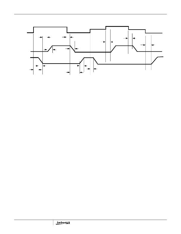
�FIGURE� 1.� TIMING� DIAGRAM�
�Operation�
�Designed� for� versatility� and� speed,� the� PX3511A� and�
�PX3511B� MOSFET� drivers� control� both� high-side� and� low-�
�side� N-Channel� FETs� of� a� half-bridge� power� train� from� one�
�externally� provided� PWM� signal.�
�Prior� to� VCC� exceeding� its� POR� level,� the� Pre-POR�
�overvoltage� protection� function� is� activated� during� initial�
�startup;� the� upper� gate� (UGATE)� is� held� low� and� the� lower�
�gate� (LGATE),� controlled� by� the� Pre-POR� overvoltage�
�protection� circuits,� is� connected� to� the� PHASE.� Once� the�
�VCC� voltage� surpasses� the� VCC� Rising� Threshold� (See�
�Electrical� Specifications),� the� PWM� signal� takes� control� of�
�gate� transitions.� A� rising� edge� on� PWM� initiates� the� turn-off�
�of� the� lower� MOSFET� (see� Timing� Diagram).� After� a� short�
�propagation� delay� [t� PDLL� ],� the� lower� gate� begins� to� fall.�
�Typical� fall� times� [t� FL� ]� are� provided� in� the� Electrical�
�Specifications� section.� Adaptive� shoot-through� circuitry�
�monitors� the� LGATE� voltage� and� determines� the� upper� gate�
�delay� time� [t� PDHU� ].� This� prevents� both� the� lower� and� upper�
�MOSFETs� from� conducting� simultaneously.� Once� this� delay�
�period� is� complete,� the� upper� gate� drive� begins� to� rise� [t� RU� ]�
�and� the� upper� MOSFET� turns� on.�
�A� falling� transition� on� PWM� results� in� the� turn-off� of� the� upper�
�MOSFET� and� the� turn-on� of� the� lower� MOSFET.� A� short�
�propagation� delay� [t� PDLU� ]� is� encountered� before� the� upper�
�gate� begins� to� fall� [t� FU� ].� Again,� the� adaptive� shoot-through�
�circuitry� determines� the� lower� gate� delay� time,� t� PDHL� .� The�
�PHASE� voltage� and� the� UGATE� voltage� are� monitored,� and�
�the� lower� gate� is� allowed� to� rise� after� PHASE� drops� below� a�
�level� or� the� voltage� of� UGATE� to� PHASE� reaches� a� level�
�depending� upon� the� current� direction� (See� next� section� for�
�details).� The� lower� gate� then� rises� [t� RL� ],� turning� on� the� lower�
�MOSFET.�
�6�
�Adaptive� Zero� Shoot-Through� Deadtime� Control�
�These� drivers� incorporate� an� adaptive� deadtime� control�
�technique� to� minimize� deadtime,� resulting� in� high� efficiency�
�from� the� reduced� freewheeling� time� of� the� lower� MOSFETs’�
�body-diode� conduction,� and� to� prevent� the� upper� and� lower�
�MOSFETs� from� conducting� simultaneously.� This� is�
�accomplished� by� ensuring� either� rising� gate� turns� on� its�
�MOSFET� with� minimum� and� sufficient� delay� after� the� other�
�has� turned� off.�
�During� turn-off� of� the� lower� MOSFET,� the� LGATE� voltage� is�
�monitored� until� it� drops� below� 1.75V,� at� which� time� the�
�UGATE� is� released� to� rise� after� 20ns� of� propagation� delay.�
�Once� the� PHASE� is� high,� the� adaptive� shoot-through�
�circuitry� monitors� the� PHASE� and� UGATE� voltages� during� a�
�PWM� falling� edge� and� the� subsequent� UGATE� turn-off.� If�
�either� the� UGATE� falls� to� less� than� 1.75V� above� the� PHASE�
�or� the� PHASE� falls� to� less� than� +0.8V,� the� LGATE� is�
�released� to� turn� on.�
�Three-State� PWM� Input�
�A� unique� feature� of� these� drivers� and� other� Intersil� drivers� is�
�the� addition� of� a� shutdown� window� to� the� PWM� input.� If� the�
�PWM� signal� enters� and� remains� within� the� shutdown� window�
�for� a� set� holdoff� time,� the� driver� outputs� are� disabled� and�
�both� MOSFET� gates� are� pulled� and� held� low.� The� shutdown�
�state� is� removed� when� the� PWM� signal� moves� outside� the�
�shutdown� window.� Otherwise,� the� PWM� rising� and� falling�
�thresholds� outlined� in� the� ELECTRICAL� SPECIFICATIONS�
�determine� when� the� lower� and� upper� gates� are� enabled.�
�This� feature� helps� prevent� a� negative� transient� on� the� output�
�voltage� when� the� output� is� shut� down,� eliminating� the�
�Schottky� diode� that� is� used� in� some� systems� for� protecting�
�the� load� from� reversed� output� voltage� events.�
�In� addition,� more� than� 400mV� hysteresis� also� incorporates�
�into� the� three-state� shutdown� window� to� eliminate� PWM�
�FN6462.0�
�February� 26,� 2007�
�相关PDF资料 |
PDF描述 |
|---|---|
| GSM08DRES | CONN EDGECARD 16POS .156 EYELET |
| T95Z226K020ESSL | CAP TANT 22UF 20V 10% 2910 |
| MAX8631YETI+T | IC LED DRVR WHITE BCKLGT 28-TQFN |
| RGM40DTBH-S189 | CONN EDGECARD 80POS R/A .156 SLD |
| BYW27-200GP-E3/73 | DIODE 1A 200V STD DO-204AL |
相关代理商/技术参数 |
参数描述 |
|---|---|
| PX3511BDDG | 功能描述:IC DRVR SYNC BUCK HF 10-DFN RoHS:是 类别:集成电路 (IC) >> PMIC - MOSFET,电桥驱动器 - 外部开关 系列:- 标准包装:50 系列:- 配置:高端 输入类型:非反相 延迟时间:200ns 电流 - 峰:250mA 配置数:1 输出数:1 高端电压 - 最大(自引导启动):600V 电源电压:12 V ~ 20 V 工作温度:-40°C ~ 125°C 安装类型:通孔 封装/外壳:8-DIP(0.300",7.62mm) 供应商设备封装:8-DIP 包装:管件 其它名称:*IR2127 |
| PX3511BDDG-RA | 功能描述:IC DRVR SYNC BUCK HF 10-DFN RoHS:是 类别:集成电路 (IC) >> PMIC - MOSFET,电桥驱动器 - 外部开关 系列:- 标准包装:6,000 系列:* |
| PX3511D | 制造商:INTERSIL 制造商全称:Intersil Corporation 功能描述:Advanced Synchronous Rectified Buck MOSFET Driver with Protection Features |
| PX3511DDDG-RA | 功能描述:IC DRVR SYNC BUCK HF 10-DFN RoHS:是 类别:集成电路 (IC) >> PMIC - MOSFET,电桥驱动器 - 外部开关 系列:- 标准包装:6,000 系列:* |
| PX3515BDDGR4XTMA1 | 制造商:Infineon Technologies AG 功能描述: 制造商:Infineon Technologies AG 功能描述:LV IC - Tape and Reel |
发布紧急采购,3分钟左右您将得到回复。