- 您现在的位置:买卖IC网 > PDF目录102828 > Q83C154DCXXX-25 (ATMEL CORP) 8-BIT, MROM, 25 MHz, MICROCONTROLLER, CQFP44 PDF资料下载
参数资料
| 型号: | Q83C154DCXXX-25 |
| 厂商: | ATMEL CORP |
| 元件分类: | 微控制器/微处理器 |
| 英文描述: | 8-BIT, MROM, 25 MHz, MICROCONTROLLER, CQFP44 |
| 封装: | CERAMIC, QFP-44 |
| 文件页数: | 84/242页 |
| 文件大小: | 3080K |
| 代理商: | Q83C154DCXXX-25 |
第1页第2页第3页第4页第5页第6页第7页第8页第9页第10页第11页第12页第13页第14页第15页第16页第17页第18页第19页第20页第21页第22页第23页第24页第25页第26页第27页第28页第29页第30页第31页第32页第33页第34页第35页第36页第37页第38页第39页第40页第41页第42页第43页第44页第45页第46页第47页第48页第49页第50页第51页第52页第53页第54页第55页第56页第57页第58页第59页第60页第61页第62页第63页第64页第65页第66页第67页第68页第69页第70页第71页第72页第73页第74页第75页第76页第77页第78页第79页第80页第81页第82页第83页当前第84页第85页第86页第87页第88页第89页第90页第91页第92页第93页第94页第95页第96页第97页第98页第99页第100页第101页第102页第103页第104页第105页第106页第107页第108页第109页第110页第111页第112页第113页第114页第115页第116页第117页第118页第119页第120页第121页第122页第123页第124页第125页第126页第127页第128页第129页第130页第131页第132页第133页第134页第135页第136页第137页第138页第139页第140页第141页第142页第143页第144页第145页第146页第147页第148页第149页第150页第151页第152页第153页第154页第155页第156页第157页第158页第159页第160页第161页第162页第163页第164页第165页第166页第167页第168页第169页第170页第171页第172页第173页第174页第175页第176页第177页第178页第179页第180页第181页第182页第183页第184页第185页第186页第187页第188页第189页第190页第191页第192页第193页第194页第195页第196页第197页第198页第199页第200页第201页第202页第203页第204页第205页第206页第207页第208页第209页第210页第211页第212页第213页第214页第215页第216页第217页第218页第219页第220页第221页第222页第223页第224页第225页第226页第227页第228页第229页第230页第231页第232页第233页第234页第235页第236页第237页第238页第239页第240页第241页第242页
174
2588F–AVR–06/2013
ATtiny261/461/861
After RESET is set low, the Programming Enable instruction needs to be executed first before
program/erase operations can be executed.
Note:
In Table 18-9, above, the pin mapping for SPI programming is listed. Not all parts use the SPI pins
dedicated for the internal SPI interface.
When programming the EEPROM, an auto-erase cycle is built into the self-timed programming
operation (in the Serial mode ONLY) and there is no need to first execute the Chip Erase
instruction. The Chip Erase operation turns the content of every memory location in both the
Program and EEPROM arrays into 0xFF.
Depending on CKSEL Fuses, a valid clock must be present. The minimum low and high periods
for the serial clock (SCK) input are defined as follows:
Low:> 2 CPU clock cycles for f
ck < 12 MHz, 3 CPU clock cycles for fck >= 12 MHz
High:> 2 CPU clock cycles for f
ck < 12 MHz, 3 CPU clock cycles for fck >= 12 MHz
18.6.1
Serial Programming Algorithm
When writing serial data to the ATtiny261/461/861, data is clocked on the rising edge of SCK.
When reading, data is clocked on the falling edge of SCK. See Figure 19-4 and Figure 19-5 for
timing details.
To program and verify the ATtiny261/461/861 in the Serial Programming mode, the following
sequence is recommended (see four byte instruction formats in Table 18-11):
1.
Power-up sequence:
Apply power between V
CC and GND while RESET and SCK are set to “0”. In some sys-
tems, the programmer can not guarantee that SCK is held low during power-up. In this
case, RESET must be given a positive pulse after SCK has been set to '0'. The duration
of the pulse must be at least t
RST (the minimum pulse width on RESET pin, see Table
19-4 on page 190) plus two CPU clock cycles.
2.
Wait for at least 20 ms and enable serial programming by sending the Programming
Enable serial instruction to pin MOSI.
3.
The serial programming instructions will not work if the communication is out of syn-
chronization. When in sync. the second byte (0x53), will echo back when issuing the
third byte of the Programming Enable instruction. Whether the echo is correct or not, all
four bytes of the instruction must be transmitted. If the 0x53 did not echo back, give
RESET a positive pulse and issue a new Programming Enable command.
4.
The Flash is programmed one page at a time. The memory page is loaded one byte at
a time by supplying the 5 LSB of the address and data together with the Load Program
memory Page instruction. To ensure correct loading of the page, the data low byte must
be loaded before data high byte is applied for a given address. The Program memory
Page is stored by loading the Write Program memory Page instruction with the 6 MSB
of the address. If polling (RDY/BSY) is not used, the user must wait at least t
WD_FLASH
before issuing the next page. (See Table 18-10.) Accessing the serial programming
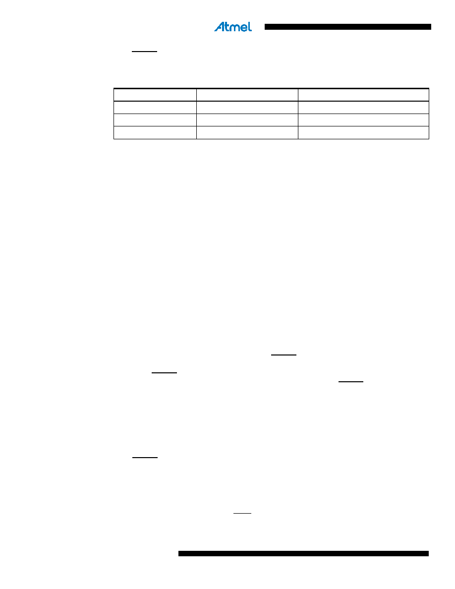
Table 18-9.
Pin Mapping Serial Programming
Symbol
Pins
I/O
Description
MOSI
PB0
I
Serial Data in
MISO
PB1
O
Serial Data out
SCK
PB2
I
Serial Clock
相关PDF资料 |
PDF描述 |
|---|---|
| Q83C154DTXXX-30D | 8-BIT, MROM, 30 MHz, MICROCONTROLLER, CQFP44 |
| Q80C32-30SHXXX:RD | 8-BIT, 30 MHz, MICROCONTROLLER, CQFP44 |
| Q80C32-36:R | 8-BIT, 36 MHz, MICROCONTROLLER, CQFP44 |
| Q80C32-44SHXXX:RD | 8-BIT, 44 MHz, MICROCONTROLLER, CQFP44 |
| Q80C32E-25:RD | 8-BIT, 25 MHz, MICROCONTROLLER, CQFP44 |
相关代理商/技术参数 |
参数描述 |
|---|---|
| Q-840 | 制造商:Qualtek Electronics Corporation 功能描述:Nema St Blade Twist Lock |
| Q-842 | 制造商:Qualtek Electronics Corporation 功能描述:NEMA TWIST-LOCK 制造商:Qualtek Electronics Corporation 功能描述:Nema St Blade Twist Lock |
| Q-844 | 制造商:Qualtek Electronics Corporation 功能描述:NEMA TWIST-LOCK 制造商:Qualtek Electronics Corporation 功能描述:Nema St Blade Twist Lock |
| Q-846 | 制造商:Qualtek Electronics Corporation 功能描述:NEMA TWIST-LOCK 制造商:Qualtek Electronics Corporation 功能描述:Nema St Blade Twist Lock |
| Q-848 | 制造商:Qualtek Electronics Corporation 功能描述:NEMA TWIST-LOCK 制造商:Qualtek Electronics Corporation 功能描述:Nema St Blade Twist Lock |
发布紧急采购,3分钟左右您将得到回复。