- 您现在的位置:买卖IC网 > PDF目录191950 > QS5930-66TQ (INTEGRATED DEVICE TECHNOLOGY INC) 5930 SERIES, PLL BASED CLOCK DRIVER, 6 TRUE OUTPUT(S), 0 INVERTED OUTPUT(S), PDSO20 PDF资料下载
参数资料
| 型号: | QS5930-66TQ |
| 厂商: | INTEGRATED DEVICE TECHNOLOGY INC |
| 元件分类: | Clock Driver |
| 英文描述: | 5930 SERIES, PLL BASED CLOCK DRIVER, 6 TRUE OUTPUT(S), 0 INVERTED OUTPUT(S), PDSO20 |
| 封装: | QSOP-20 |
| 文件页数: | 1/6页 |
| 文件大小: | 67K |
| 代理商: | QS5930-66TQ |
1
INDUSTRIALTEMPERATURERANGE
QS5930T
LOW SKEW CMOS PLL CLOCK DRIVER WITH INTEGRATED LOOP FILTER
R
D
Q
Q0
R
D
Q
Q1
R
D
Q
Q2
R
D
Q
Q3
R
D
Q
Q4
R
D
Q
Q/2
0
1
0
/2
VCO
LOO P
FILTER
PH AS E
DETE CTO R
FREQ _SEL
FEED BACK
SYNC
PLL_EN
OE/RST
Q
SEPTEMBER 2000
2000
Integrated Device Technology, Inc.
DSC-5849/1
c
QS5930T
INDUSTRIAL TEMPERATURE RANGE
LOW SKEW CMOS PLL
CLOCK DRIVER WITH
INTEGRATED LOOP FILTER
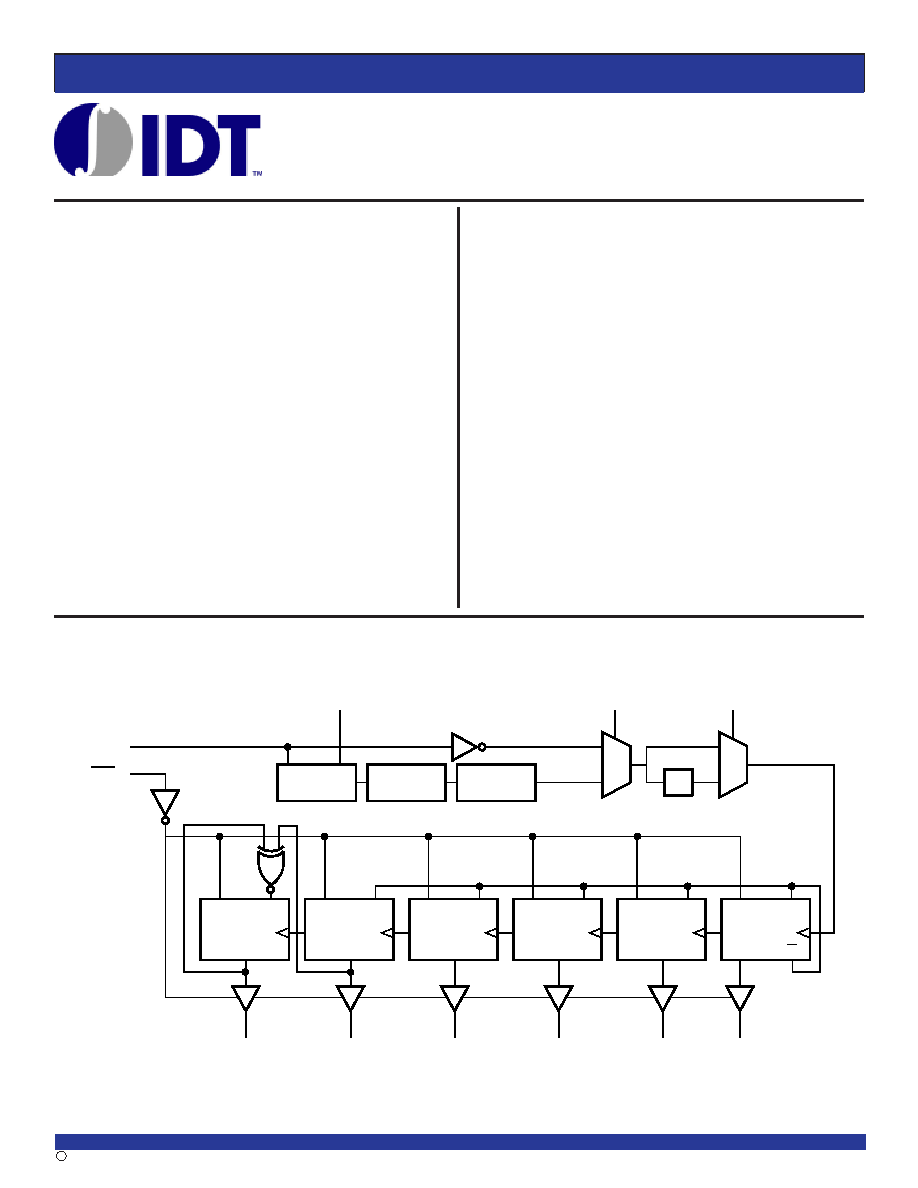
FUNCTIONAL BLOCK DIAGRAM
FEATURES:
5V operation
Q/2 output, 5 Q outputs
Useful for Pentium, PowerPC, and PCI systems
Internal loop filter RC network
Low noise TTL level outputs
<250ps rising edge output skew
Balanced drive outputs ±24mA
PLL bypass feature for low frequency testing
Internal VCO/2 option for wider frequency range
Outputs tri-state and reset while OE/
RST is low
ESD > 2000V
Latch up > -300mA
Available in QSOP package
DESCRIPTION
The QS5930T Clock Driver uses an internal phase locked loop
(PLL) to lock low skew outputs to a reference clock input. Six outputs
are available: Q0–Q4, Q/2. Careful layout and design ensure < 250ps
skew between the Q0–Q4, and Q/2 outputs. The QS5930T includes
an internal RC filter which provides excellent jitter characteristics and
eliminates the need for external components. Various combinations of
feedback and a divide-by-2 in the VCO path allow applications to be
customized for linear VCO operation over a wide range of input SYNC
frequencies. The PLL can also be disabled by the PLL_EN signal to
allow low frequency or DC testing. The QS5930T is designed for use
in cost sensitive high-performance computing systems, workstations,
multi-board computers, networking hardware, and mainframe sys-
tems. Several can be used in parallel or scattered throughout a sys-
tem for guaranteed low skew, system-wide clock distribution networks.
In the QSOP package, the QS5930T clock driver represents the best
value in small form factor, high-performance clock management prod-
ucts.
For more information on PLL clock driver products, see Application
Note AN-227.
相关PDF资料 |
PDF描述 |
|---|---|
| QS762470-55J | 1 CHANNEL(S), LOCAL AREA NETWORK CONTROLLER, PQCC44 |
| QSC112.C4A0 | PHOTO TRANSISTOR DETECTOR |
| QSC114.C6A0 | PHOTO TRANSISTOR DETECTOR |
| QSD123.A4A0 | PHOTO TRANSISTOR DETECTOR |
| QSD128.A4R0 | PHOTO TRANSISTOR DETECTOR |
相关代理商/技术参数 |
参数描述 |
|---|---|
| QS5930T | 制造商:IDT 制造商全称:Integrated Device Technology 功能描述:LOW SKEW CMOS PLL CLOCK DRIVER WITH INTEGRATED LOOP FILTER |
| QS5931-50Q | 制造商:未知厂家 制造商全称:未知厂家 功能描述:Six Distributed-Output Clock Driver |
| QS5931-66Q | 制造商:未知厂家 制造商全称:未知厂家 功能描述:Six Distributed-Output Clock Driver |
| QS5931-80Q | 制造商:未知厂家 制造商全称:未知厂家 功能描述:Six Distributed-Output Clock Driver |
| QS5931Q | 制造商:未知厂家 制造商全称:未知厂家 功能描述:SIX DISTRIBUTED-OUTPUT CLOCK DRIVER|CMOS|SSOP|20PIN|PLASTIC |
发布紧急采购,3分钟左右您将得到回复。