参数资料
| 型号: | QT60240-ATG |
| 厂商: | Atmel |
| 文件页数: | 21/26页 |
| 文件大小: | 0K |
| 描述: | IC TOUCH SENSOR 24KEY 32-TQFP |
| 标准包装: | 3,000 |
| 系列: | QMatrix™ |
| 类型: | 电容性 |
| 输入数/键: | 24 键 |
| 分辨率(位): | 10 b |
| 评估套件: | 可供 |
| 数据接口: | I²C,串行,SPI? |
| 电压基准: | 外部 |
| 电源电压: | 1.8V,3.3V,5V |
| 电流 - 电源: | 4.6mA |
| 工作温度: | -40°C ~ 85°C |
| 安装类型: | 表面贴装 |
| 封装/外壳: | 32-TQFP |
| 供应商设备封装: | 32-TQFP |
| 包装: | 带卷 (TR) |
| 其它名称: | QT60240-ATG-ND QT60240-ATGTR |
The Cs should be connected as shown in Figure 2.7, page 9.
The value of these capacitors is not critical but 4.7nF is
recommended for most cases. They should be 10 percent
X7R ceramics. If the transverse capacitive coupling from X to
Y is large enough the voltage on a Cs capacitor can saturate,
destroying gain. In such cases the burst length should be
reduced and/or the Cs value increased. See Section 2.4.
If a Y line is not used its corresponding Cs capacitor may be
omitted and the pins left floating.
2.4 Sample Capacitor Saturation
Cs voltage saturation at a pin YnB is shown in Figure 2.1
Saturation begins to occur when the voltage at a YnB pin
becomes more negative than -0.25V at the end of the burst.
This nonlinearity is caused by excessive voltage
accumulation on Cs inducing conduction in the pin protection
diodes. This badly saturated signal destroys key gain and
introduces a strong thermal coefficient which can cause
'phantom' detection. The cause of this is either from the burst
length being too long, the Cs value being too small, or the
X-Y transfer coupling being too large. Solutions include
loosening up the key structure interleaving, more separation
of the X and Y lines on the PCB, increasing Cs, and
decreasing the burst length.
Increasing Cs will make the part slower; decreasing burst
length will make it less sensitive. A better PCB layout and a
looser key structure (up to a point) have no negative effects.
Cs voltages should be observed on an oscilloscope with the
matrix layer bonded to the panel material; if the Rs side of
any Cs ramps more negative than -0.25 volts during any burst
(not counting overshoot spikes which are probe artifacts),
there is a potential saturation problem.
Figure 2.2 shows a defective waveform similar to that of 2.1,
but in this case the distortion is caused by excessive stray
capacitance coupling from the Y line to AC ground ; for
example, from running too near and too far alongside a
ground trace, ground plane, or other traces. The excess
coupling causes the charge-transfer effect to dissipate a
significant portion of the received charge from a key into the
stray capacitance. This phenomenon is more subtle; it can be
best detected by increasing BL to a high count and watching
what the waveform does as it descends towards and below
-0.25V. The waveform will appear deceptively straight, but it
will slowly start to flatten even before the -0.25V level is
reached.
A correct waveform is shown in Figure 2.3. Note that the
bottom edge of the bottom trace is substantially straight
(ignoring the downward spikes).
Unlike other QT circuits, the Cs capacitor values on QT60xx 0
devices have no effect on conversion gain. However , they do
affect conversion time.
Unused Y lines should be left open.
2.5 Sample Resistors
There are three sample resistors (Rs) used to perform
single-slope ADC conversion of the acquired charge on each
Cs capacitor. These resistors directly control acquisition gain;
larger values of Rs will proportionately increase signal gain.
For most applications Rs should be 1M
. Unused Y lines do
not require an Rs resistor.
2.6 Signal Levels
Quantum’s QmBtn software makes it is easy to observe the
absolute level of signal received by the sensor on each key.
The signal values should normally be in the range of 200 to
750 counts with properly designed key shapes and values of
Rs. However, long adjacent runs of X and Y lines can also
artificially boost the signal values, and induce signal
saturation; this is to be avoided. The X-to-Y coupling should
come mostly from intra-key electrode coupling, not from stray
X-to-Y trace coupling.
lQ
4
QT60240-ISG R8.06/0906
Figure 2.1 VCs - Nonlinear During Burst
(Burst too long, or Cs too small, or X-Y transcapacitance too large)
Figure 2.2 VCs - Poor Gain, Nonlinear During Burst
(Excess capacitance from Y line to Gnd)
Figure 2.3 VCs - Correct
X Drive
YnB
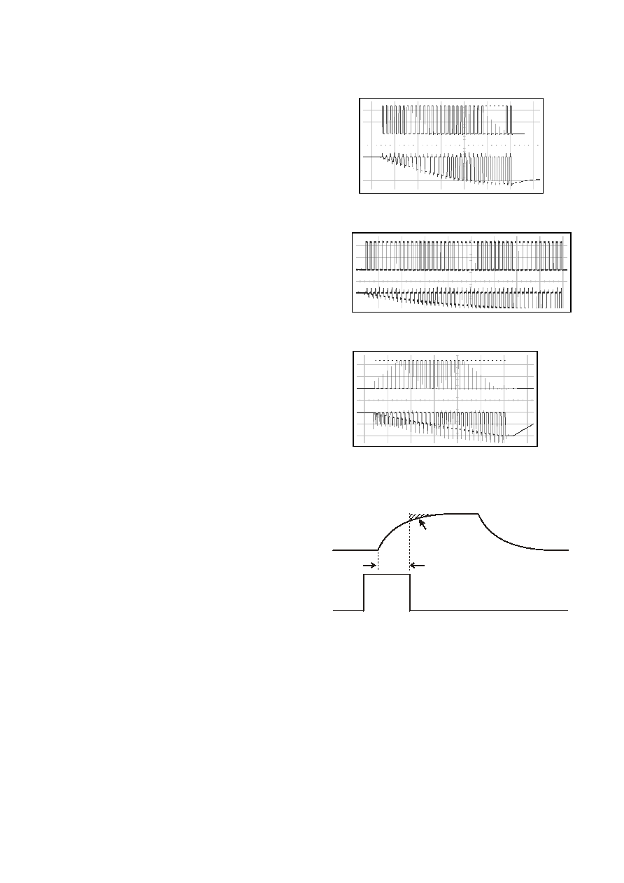
Figure 2.4 X-Drive Pulse Roll-off and Dwell Time
The Dwell time is fixed at ~500ns - see Section 2.7
X drive
Lost charge due to
inadequate settling
before end of dwell time
Y gate
Dwell time
X Drive
YnB
X Drive
YnB
相关PDF资料 |
PDF描述 |
|---|---|
| MS27472T24B35SA | CONN RCPT 128POS WALL MNT W/SCKT |
| VI-JWN-MX-F4 | CONVERTER MOD DC/DC 18.5V 75W |
| VI-200-MX-F1 | CONVERTER MOD DC/DC 5V 75W |
| VI-B5Y-IU-B1 | CONVERTER MOD DC/DC 3.3V 132W |
| VI-JWN-MX-F1 | CONVERTER MOD DC/DC 18.5V 75W |
相关代理商/技术参数 |
参数描述 |
|---|---|
| QT60240-ATG SL924 | 制造商:Atmel Corporation 功能描述:INTEGRATED-CIRCUIT 制造商:Atmel 功能描述:INTEGRATED-CIRCUIT |
| QT60240-ATG-SL924 | 功能描述:接口 - 专用 Integrated Circuit RoHS:否 制造商:Texas Instruments 产品类型:1080p60 Image Sensor Receiver 工作电源电压:1.8 V 电源电流:89 mA 最大功率耗散: 最大工作温度:+ 85 C 安装风格:SMD/SMT 封装 / 箱体:BGA-59 |
| QT60240-ISG | 功能描述:接口 - 专用 1.8 - 5.5V 24 Chan QMatrix RoHS:否 制造商:Texas Instruments 产品类型:1080p60 Image Sensor Receiver 工作电源电压:1.8 V 电源电流:89 mA 最大功率耗散: 最大工作温度:+ 85 C 安装风格:SMD/SMT 封装 / 箱体:BGA-59 |
| QT60240-ISG QS130 | 功能描述:SENSOR IC MTRX TOUCH24KEY 32-QFN RoHS:是 类别:集成电路 (IC) >> 数据采集 - 触摸屏控制器 系列:QMatrix™ 标准包装:96 系列:- 类型:- 触摸面板接口:- 输入数/键:- 分辨率(位):- 评估套件:* 数据接口:- 数据速率/采样率 (SPS,BPS):- 电压基准:- 电源电压:- 电流 - 电源:- 工作温度:- 安装类型:表面贴装 封装/外壳:16-TSSOP(0.173",4.40mm 宽) 供应商设备封装:16-TSSOP 包装:带卷 (TR) |
| QT60240-ISG-QS130 | 功能描述:接口 - 专用 1.8 - 5.5V 24 Chan QMatrix RoHS:否 制造商:Texas Instruments 产品类型:1080p60 Image Sensor Receiver 工作电源电压:1.8 V 电源电流:89 mA 最大功率耗散: 最大工作温度:+ 85 C 安装风格:SMD/SMT 封装 / 箱体:BGA-59 |
发布紧急采购,3分钟左右您将得到回复。