- 您现在的位置:买卖IC网 > PDF目录4509 > R1EX25002ATA00A#S0 (Renesas Electronics America)IC EEPROM 2K 5MHZ 8TSSOP PDF资料下载
参数资料
| 型号: | R1EX25002ATA00A#S0 |
| 厂商: | Renesas Electronics America |
| 文件页数: | 15/24页 |
| 文件大小: | 0K |
| 描述: | IC EEPROM 2K 5MHZ 8TSSOP |
| 标准包装: | 1 |
| 格式 - 存储器: | EEPROMs - 串行 |
| 存储器类型: | EEPROM |
| 存储容量: | 2K (256 x 8) |
| 速度: | 3MHz,5MHz |
| 接口: | SPI 串行 |
| 电源电压: | 1.8 V ~ 5.5 V |
| 工作温度: | -40°C ~ 85°C |
| 封装/外壳: | 8-TSSOP(0.173",4.40mm 宽) |
| 供应商设备封装: | 8-TSSOP |
| 包装: | 标准包装 |
| 其它名称: | R1EX25002ATA00A#S0DKR |
�� �
�
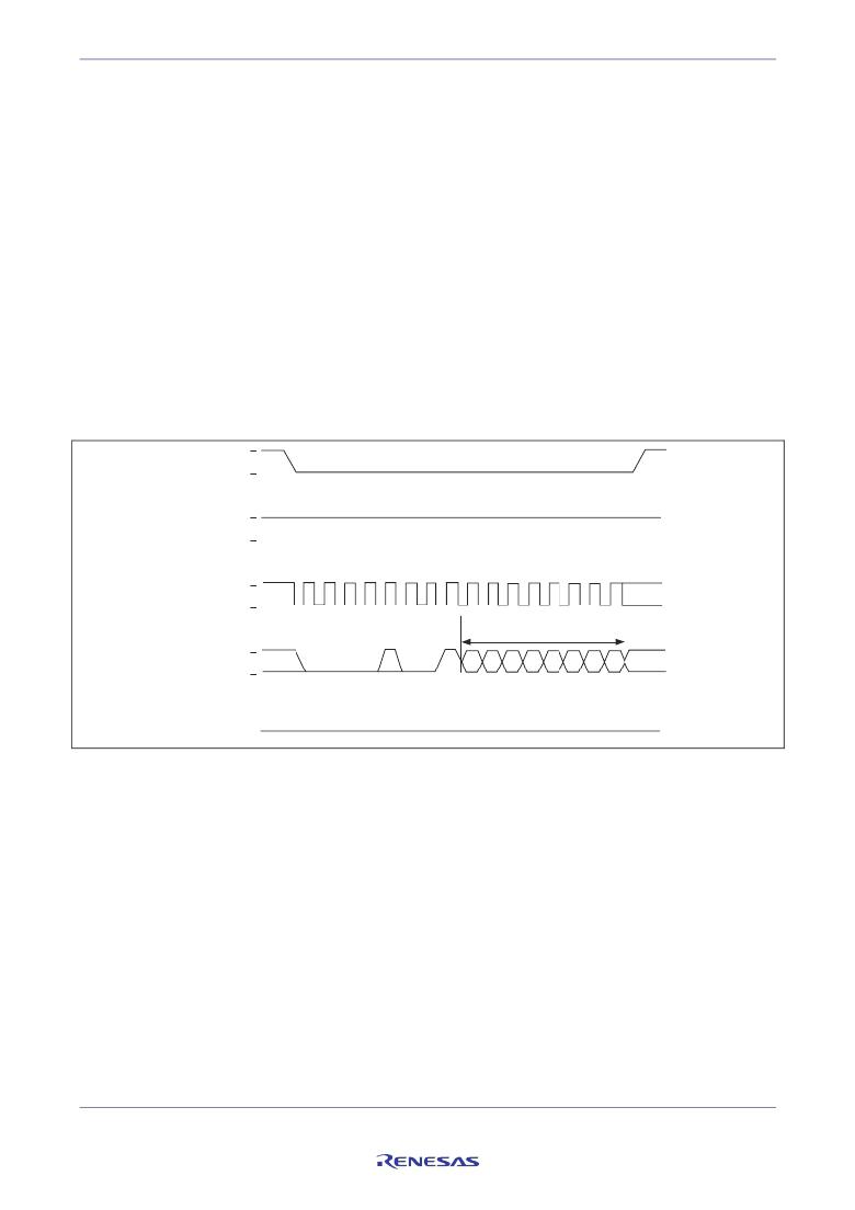
�R1EX25002Axx00A/R1EX25004Axx00A�
�Write� Status� Register� (WRSR):�
�The� Write� Status� Register� (WRSR)� instruction� allows� new� values� to� be� written� to� the� Status� Register.� Before� it� can� be�
�accepted,� a� Write� Enable� (WREN)� instruction� must� previously� have� been� executed.� After� the� Write� Enable� (WREN)�
�instruction� has� been� decoded� and� executed,� the� device� sets� the� Write� Enable� Latch(WEL).� The� instruction� sequence� is�
�shown� in� the� following� figure.� The� Write� Status� Register� (WRSR)� instruction� has� no� effect� on� b6,� b5,� b4,� b1� and� b0� of�
�the� Status� Register.� b6,� b5� and� b4� are� always� read� as� 0.� Chip� select� (� S� )� must� be� driven� high� after� the� rising� edge� of�
�serial� clock� (C)� that� latches� in� the� eighth� bit� of� the� data� byte,� and� before� the� next� rising� edge� of� serial� clock� (C).�
�Otherwise,� the� Write� Status� Register� (WRSR)� instruction� is� not� executed.� As� soon� as� chip� select� (� S� )� is� driven� high,� the�
�self-timed� Write� Status� Register� cycle� (whose� duration� is� t� W� )� is� initiated.� While� the� Write� Status� Register� cycle� is� in�
�progress,� the� Status� Register� may� still� be� read� to� check� the� value� of� the� Write� In� Progress� (WIP)� bit.� The� Write� In�
�Progress� (WIP)� bit� is� 1� during� the� self-timed� Write� Status� Register� cycle,� and� is� 0� when� it� is� completed.� When� the�
�cycle� is� completed,� Write� Enable� Latch(WEL)� is� reset.� The� Write� Status� Register� (WRSR)� instruction� allows� the� user�
�to� change� the� values� of� the� Block� Protect� (BP1,� BP0)� bits,� to� define� the� size� of� the� area� that� is� to� be� treated� as� read-only,�
�as� defined� in� the� Status� Register� Format� table.�
�The� contents� of� Block� Protect� (BP1,� BP0)� bits� are� frozen� at� their� current� values� just� before� the� start� of� the� execution� of�
�the� Write� Status� Register� (WRSR)� instruction.� The� new,� updated� values� take� effect� at� the� moment� of� completion� of� the�
�execution� of� Write� Status� Register� (WRSR)� instruction.�
�Write� Status� Register� (WRSR)� Sequence�
�S�
�W�
�V� IH�
�V� IL�
�V� IH�
�V� IL�
�0�
�1�
�2�
�3�
�4�
�5�
�6�
�7�
�8�
�9�
�10� 11� 12� 13� 14�
�15�
�C�
�V� IH�
�V� IL�
�Status� Register� In�
�D�
�V� IH�
�V� IL�
�7�
�MSB�
�6�
�5�
�4�
�3�
�2�
�1�
�0�
�Q�
�REJ03C0357-0002� Rev.� 0.02� Jan.14� .2009�
�page� 13� of� 20�
�High-Z�
�相关PDF资料 |
PDF描述 |
|---|---|
| EP4CGX15BF14C6N | IC CYCLONE IV FPGA 15K 169 FBGA |
| A3P400-1PQG208 | IC FPGA 1KB FLASH 400K 208-PQFP |
| M1A3P400-1PQG208 | IC FPGA 1KB FLASH 400K 208-PQFP |
| R1EX24008ATAS0A#S0 | IC EEPROM 8K 400KHZ 8TSSOP |
| M1A3P400-1PQ208 | IC FPGA 1KB FLASH 400K 208-PQFP |
相关代理商/技术参数 |
参数描述 |
|---|---|
| R1EX25002ATA00G | 制造商:RENESAS 制造商全称:Renesas Technology Corp 功能描述:Serial Peripheral Interface 2k EEPROM 4k EEPROM |
| R1EX25002ATA00I | 制造商:RENESAS 制造商全称:Renesas Technology Corp 功能描述:Serial Peripheral Interface Electrically Erasable and Programmable Read Only Memory |
| R1EX25002ATA00I#S0 | 制造商:Renesas Electronics Corporation 功能描述:SERIAL EEPROM 2K, SPI, TSSOP8, 制造商:Renesas Electronics Corporation 功能描述:SERIAL EEPROM 2K, SPI, TSSOP8, I-GRADE - Tape and Reel 制造商:Renesas Electronics Corporation 功能描述:IC EEPROM 2KBIT 5MHZ 8TSSOP |
| R1EX25004ASA00A | 制造商:RENESAS 制造商全称:Renesas Technology Corp 功能描述:Serial Peripheral Interface Electrically Erasable and Programmable Read Only Memory |
| R1EX25004ASA00A#S0 | 功能描述:IC EEPROM 4K 5MHZ 8SOP RoHS:是 类别:集成电路 (IC) >> 存储器 系列:- 标准包装:1 系列:- 格式 - 存储器:闪存 存储器类型:闪存 - NAND 存储容量:4G(256M x 16) 速度:- 接口:并联 电源电压:2.7 V ~ 3.6 V 工作温度:0°C ~ 70°C 封装/外壳:48-TFSOP(0.724",18.40mm 宽) 供应商设备封装:48-TSOP I 包装:Digi-Reel® 其它名称:557-1461-6 |
发布紧急采购,3分钟左右您将得到回复。