- 您现在的位置:买卖IC网 > PDF目录380636 > R1Q2A3618ABG-50R (Renesas Technology Corp.) 36-Mbit QDR™II SRAM 2-word Burst PDF资料下载
参数资料
| 型号: | R1Q2A3618ABG-50R |
| 厂商: | Renesas Technology Corp. |
| 英文描述: | 36-Mbit QDR™II SRAM 2-word Burst |
| 文件页数: | 14/25页 |
| 文件大小: | 394K |
| 代理商: | R1Q2A3618ABG-50R |
R1Q2A3636/R1Q2A3618/R1Q2A3609
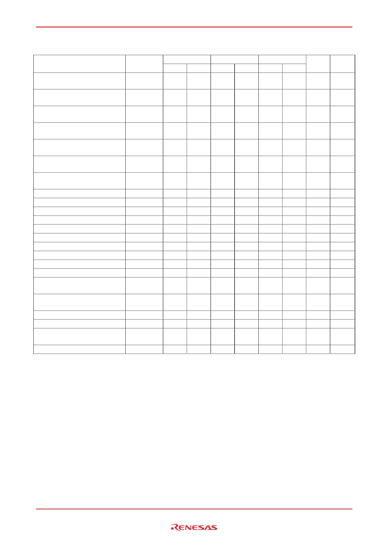
AC Characteristics
(Ta = 0 to +70
°
C, V
DD
= 1.8V
±
0.1V)
60
Max
Min
Max
6.30
6.00
8.00
40
50
Parameter
Symbol
t
KHKH
Min
4.00
Max
5.25
Min
5.00
Unit
ns
Notes
Average clock cycle time
(K, /K, C, /C)
Clock phase jitter
(K, /K, C, /C)
Clock high time
(K, /K, C, /C)
Clock low time
(K, /K, C, /C)
Clock to /clock
(K to /K, C to /C)
/Clock to clock
(/K to K, /C to C)
Clock to data clock
(K to C, /K to /C)
DLL lock time (K, C)
K static to DLL reset
C, /C high to output valid
C, /C high to output hold
C, /C high to echo clock valid
C, /C high to echo clock hold
CQ, /CQ high to output valid
CQ, /CQ high to output hold
C, /C high to output high-Z
C, /C high to output low-Z
Address valid to K, /K rising
edge
Control inputs valid to K rising
edge
Data-in valid to K, /K rising edge
K, /K rising edge to address hold
K, /K rising edge to control
inputs hold
K, /K rising edge to data-in hold
Notes: 1. This is a synchronous device. All addresses, data and control lines must meet the specified setup and hold
times for all latching clock edges.
2. V
slew rate must be less than 0.1 V DC per 50 ns for DLL lock retention. DLL lock time begins once V
DD
and input clock are stable. It is recommended that the device is kept inactive during these cycles.
3. Clock phase jitter is the variance from clock rising edge to the next expected clock rising edge.
4. Echo clock is very tightly controlled to data valid / data hold. By design, there is a ±0.1 ns variation from echo
clock to data. The datasheet parameters reflect tester guardbands and test setup variations.
5. Transitions are measured ±100 mV from steady-state voltage.
6. At any given voltage and temperature t
CHQZ
is less than t
CHQX1
and t
CHQZ
less than t
CHQV
.
7. These parameters are sampled.
Remarks:
1. Test conditions as specified with the output loading as shown in AC Test Conditions unless otherwise noted.
2. Control input signals may not be operated with pulse widths less than t
KHKL
(min).
3. If C, /C are tied high, K, /K become the references for C, /C timing parameters.
4. V
DDQ
is +1.5 V DC.
5. Control signals are /R, /W, /BW, /BW0, /BW1, /BW2 and /BW3.
BWn signals must operate at the same timing as Data in.
6. t
CHQV
, t
CHCQV
are 0.65 ns and t
CHQX
, t
CHCQX
are -0.65 ns on R1Q2A3636ABG (-40R, -50R) devices.
t
KC
var
0.20
0.20
0.20
ns
3
t
KHKL
1.60
2.00
2.40
ns
t
KLKH
1.60
2.00
2.40
ns
t
KH/KH
1.80
2.20
2.70
ns
t
/KHKH
1.80
2.20
2.70
ns
t
KHCH
0
1.10
0
1.60
0
2.10
ns
t
KC
lock
t
KC
reset
t
CHQV
t
CHQX
t
CHCQV
t
CHCQX
t
CQHQV
t
CQHQX
t
CHQZ
t
CHQX1
t
AVKH
1,024
30
0.45
0.45
0.30
0.45
0.35
0.45
0.45
0.30
0.45
1,024
30
0.45
0.45
0.35
0.45
0.40
0.45
0.45
0.35
0.45
1,024
30
0.50
0.50
0.40
0.50
0.50
0.50
0.50
0.40
0.50
Cycle
ns
ns
ns
ns
ns
ns
ns
ns
ns
ns
2
7
4, 7
4, 7
5
5
1
t
IVKH
0.35
0.40
0.50
ns
1
t
DVKH
t
KHAX
t
KHIX
0.35
0.35
0.35
0.40
0.40
0.40
0.50
0.50
0.50
ns
ns
ns
1
1
1
t
KHDX
0.35
0.40
0.50
ns
1
REJ03C0294-0003 Rev.0.03 Jul. 31, 2007
Page 14 of 23
相关PDF资料 |
PDF描述 |
|---|---|
| R1Q2A3618ABG-60R | 36-Mbit QDR™II SRAM 2-word Burst |
| R1Q2A3636 | 36-Mbit QDR™II SRAM 2-word Burst |
| R1Q2A3636ABG-40R | 36-Mbit QDR™II SRAM 2-word Burst |
| R1Q2A3636ABG-50R | 36-Mbit QDR™II SRAM 2-word Burst |
| R1Q2A3636ABG-60R | 36-Mbit QDR™II SRAM 2-word Burst |
相关代理商/技术参数 |
参数描述 |
|---|---|
| R1Q2A3618ABG50RB0 | 制造商:RENESAS 制造商全称:Renesas Technology Corp 功能描述:36-Mbit QDR?II SRAM 2-word Burst |
| R1Q2A3618ABG50RS0 | 制造商:RENESAS 制造商全称:Renesas Technology Corp 功能描述:36-Mbit QDR?II SRAM 2-word Burst |
| R1Q2A3618ABG50RT0 | 制造商:RENESAS 制造商全称:Renesas Technology Corp 功能描述:36-Mbit QDR?II SRAM 2-word Burst |
| R1Q2A3618ABG-60R | 制造商:RENESAS 制造商全称:Renesas Technology Corp 功能描述:36-Mbit QDR™II SRAM 2-word Burst |
| R1Q2A3618ABG60RB0 | 制造商:RENESAS 制造商全称:Renesas Technology Corp 功能描述:36-Mbit QDR?II SRAM 2-word Burst |
发布紧急采购,3分钟左右您将得到回复。