- 您现在的位置:买卖IC网 > PDF目录380637 > R1Q3A3636 (Renesas Technology Corp.) 36-Mbit QDR™II SRAM 4-word Burst PDF资料下载
参数资料
| 型号: | R1Q3A3636 |
| 厂商: | Renesas Technology Corp. |
| 英文描述: | 36-Mbit QDR™II SRAM 4-word Burst |
| 文件页数: | 8/26页 |
| 文件大小: | 407K |
| 代理商: | R1Q3A3636 |
R1Q3A3636/R1Q3A3618/R1Q3A3609
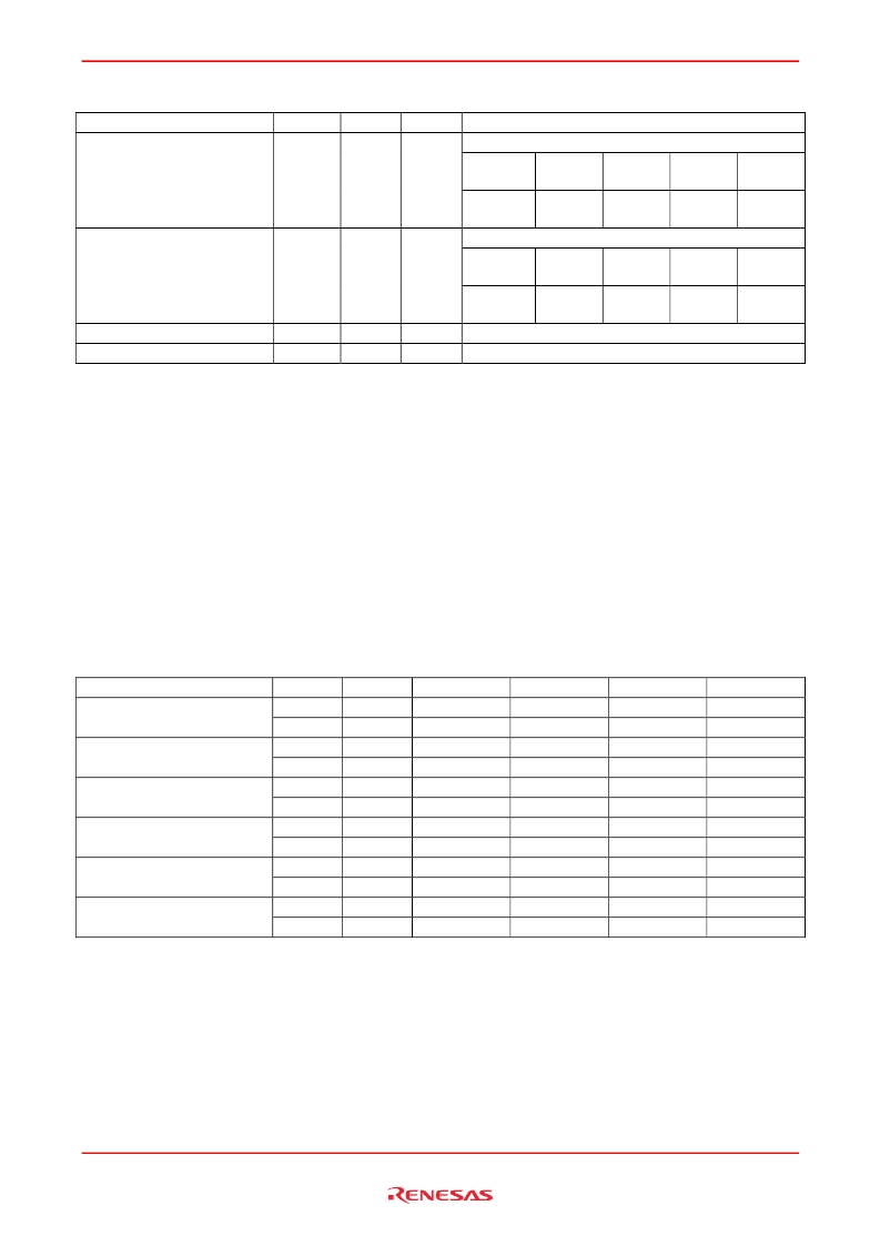
K Truth Table
Operation
K
↑
/R
H*
7
/W
L*
8
D or Q
Data in
Input
data
Output
clock
Data out
Output
data
Output
clock
D =
×
or Q = High-Z
Previous state
D(A+0)
D(A+1)
D(A+2)
D(A+3)
Write Cycle:
Load address, input write data
on consecutive K and /K rising
edges
K(t+1)
↑
/K(t+1)
↑
K(t+2)
↑
/K(t+2)
↑
Q(A+0)
Q(A+1)
Q(A+2)
Q(A+3)
Read Cycle:
Load address, output read
data on consecutive C and /C
rising edges
↑
L*
8
×
/C(t+1)
↑
C(t+2)
↑
/C(t+2)
↑
C(t+3)
↑
NOP (No operation)
Standby (Clock stopped)
Notes: 1. H: high level, L: low level,
×
: don’t care,
↑
: rising edge.
2. Data inputs are registered at K and /K rising edges. Data outputs are delivered at C and /C rising edges,
except if C and /C are high, then data outputs are delivered at K and /K rising edges.
3. /R and /W must meet setup/hold times around the rising edges (low to high) of K and are registered at the
rising edge of K.
4. This device contains circuitry that will ensure the outputs will be in high-Z during power-up.
5. Refer to state diagram and timing diagrams for clarification.
6. When clocks are stopped, the following cases are recommended; the case of K = low, /K = high, C = low and
/C = high, or the case of K = high, /K = low, C = high and /C = low. This condition is not essential, but permits
most rapid restart by overcoming transmission line charging symmetrically.
7. If this signal was low to initiate the previous cycle, this signal becomes a “don’t care” for this operation;
however, it is strongly recommended that this signal be brought high, as shown in the truth table.
8. This signal was high on previous K clock rising edge. Initiating consecutive READ or WRITE operations on
consecutive K clock rising edges is not permitted. The device will ignore the second request.
Byte Write Truth Table (x36)
↑
H
×
H
×
Stopped
Operation
K
↑
↑
↑
↑
↑
↑
/K
↑
↑
↑
↑
↑
↑
/BW0
L
L
L
L
H
H
H
H
H
H
H
H
/BW1
L
L
H
H
L
L
H
H
H
H
H
H
/BW2
L
L
H
H
H
H
L
L
H
H
H
H
/BW3
L
L
H
H
H
H
H
H
L
L
H
H
Write D0 to D35
Write D0 to D8
Write D9 to D17
Write D18 to D26
Write D27 to D35
Write nothing
Notes: 1. H: high level, L: low level,
↑
: rising edge.
2. Assumes a WRITE cycle was initiated. /BWx can be altered for any portion of the BURST WRITE operation
provided that the setup and hold requirements are satisfied.
REJ03C0295-0003 Rev.0.03 Jul. 31, 2007
Page 8 of 24
相关PDF资料 |
PDF描述 |
|---|---|
| R1Q3A3636ABG-30R | 36-Mbit QDR™II SRAM 4-word Burst |
| R1Q3A3636ABG-33R | 36-Mbit QDR™II SRAM 4-word Burst |
| R1Q3A3636ABG-40R | 36-Mbit QDR™II SRAM 4-word Burst |
| R1RP0404D | 4M High Speed SRAM (1-Mword 】 4-bit) |
| R1RP0404DGE-2LR | 4M High Speed SRAM (1-Mword 】 4-bit) |
相关代理商/技术参数 |
参数描述 |
|---|---|
| R1Q3A3636ABG-30R | 制造商:RENESAS 制造商全称:Renesas Technology Corp 功能描述:36-Mbit QDR™II SRAM 4-word Burst |
| R1Q3A3636ABG-33R | 制造商:RENESAS 制造商全称:Renesas Technology Corp 功能描述:36-Mbit QDR™II SRAM 4-word Burst |
| R1Q3A3636ABG-40R | 制造商:RENESAS 制造商全称:Renesas Technology Corp 功能描述:36-Mbit QDR™II SRAM 4-word Burst |
| R1Q3A3636ABG40RB0 | 制造商:RENESAS 制造商全称:Renesas Technology Corp 功能描述:36-Mbit QDR?II SRAM 2-word Burst |
| R1Q3A3636ABG40RS0 | 制造商:RENESAS 制造商全称:Renesas Technology Corp 功能描述:36-Mbit QDR?II SRAM 2-word Burst |
发布紧急采购,3分钟左右您将得到回复。