- 您现在的位置:买卖IC网 > PDF目录69305 > R5F21296JXXXSP 16-BIT, FLASH, 20 MHz, MICROCONTROLLER, PDSO20 PDF资料下载
参数资料
| 型号: | R5F21296JXXXSP |
| 元件分类: | 微控制器/微处理器 |
| 英文描述: | 16-BIT, FLASH, 20 MHz, MICROCONTROLLER, PDSO20 |
| 封装: | 4.40 X 6.50 MM, 0.65 MM PITCH, PLASTIC, LSSOP-20 |
| 文件页数: | 2/63页 |
| 文件大小: | 612K |
| 代理商: | R5F21296JXXXSP |
第1页当前第2页第3页第4页第5页第6页第7页第8页第9页第10页第11页第12页第13页第14页第15页第16页第17页第18页第19页第20页第21页第22页第23页第24页第25页第26页第27页第28页第29页第30页第31页第32页第33页第34页第35页第36页第37页第38页第39页第40页第41页第42页第43页第44页第45页第46页第47页第48页第49页第50页第51页第52页第53页第54页第55页第56页第57页第58页第59页第60页第61页第62页第63页
R8C/28 Group, R8C/29 Group
1. Overview
Rev.2.10
Sep 26, 2008
Page 8 of 67
REJ03B0169-0210
1.6
Pin Functions
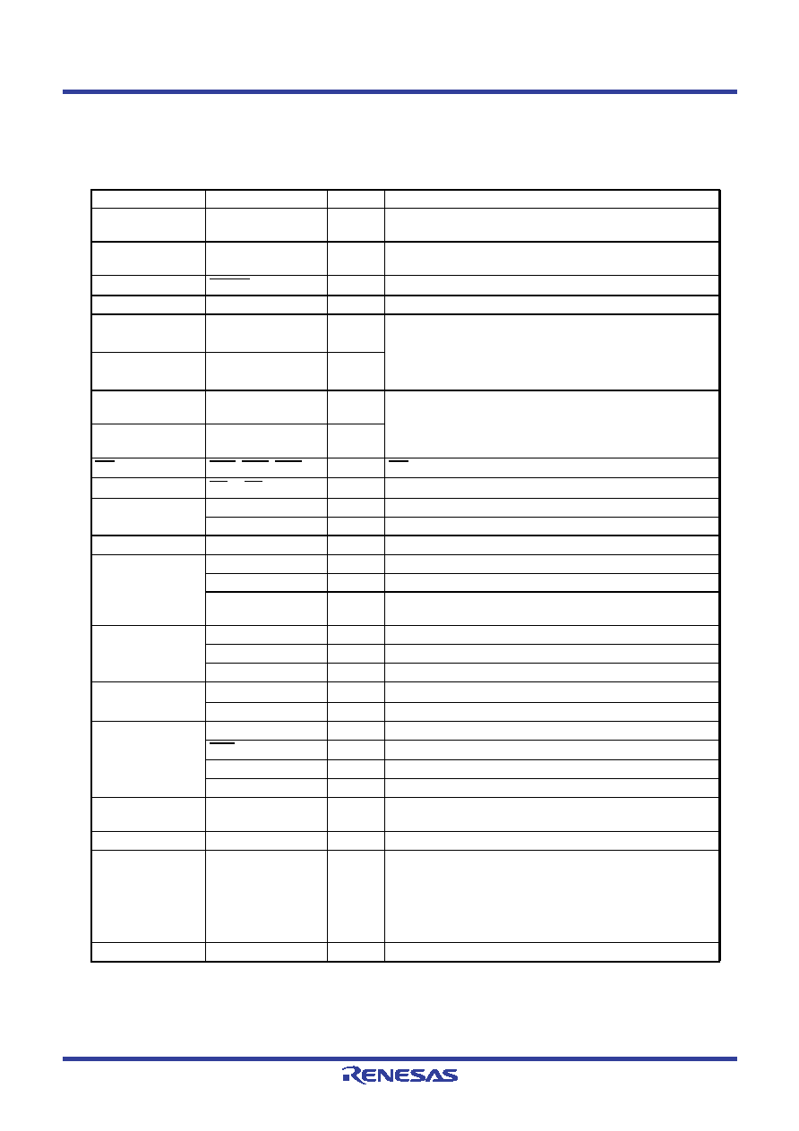
Table 1.5 lists Pin Functions.
I: Input
O: Output
I/O: Input and output
Table 1.5
Pin Functions
Type
Symbol
I/O Type
Description
Power supply input
VCC, VSS
I
Apply 2.2 to 5.5 V (J, K version are 2.7 to 5.5 V) to the VCC
pin. Apply 0 V to the VSS pin.
Analog power
supply input
AVCC, AVSS
I
Power supply for the A/D converter.
Connect a capacitor between AVCC and AVSS.
Reset input
RESET
I
Input “L” on this pin resets the MCU.
MODE
I
Connect this pin to VCC via a resistor.
XIN clock input
XIN
I
These pins are provided for XIN clock generation circuit I/O.
Connect a ceramic resonator or a crystal oscillator between
the XIN and XOUT pins. To use an external clock, input it to
the XIN pin and leave the XOUT pin open.
XIN clock output
XOUT
O
XCIN clock input
(N, D version)
XCIN
I
These pins are provided for XCIN clock generation circuit I/O.
Connect a crystal oscillator between the XCIN and XCOUT
pins. To use an external clock, input it to the XCIN pin and
leave the XCOUT pin open.
XCIN clock output
(N, D version)
XCOUT
O
INT interrupt input
INT0, INT1, INT3
IINT interrupt input pins
Key input interrupt
KI0 to KI3
I
Key input interrupt input pins
Timer RA
TRAO
O
Timer RA output pin
TRAIO
I/O
Timer RA I/O pin
Timer RB
TRBO
O
Timer RB output pin
Timer RC
TRCCLK
I
External clock input pin
TRCTRG
I
External trigger input pin
TRCIOA, TRCIOB,
TRCIOC, TRCIOD
I/O
Sharing output-compare output / input-capture input / PWM /
PWM2 output pins
Serial interface
CLK0
I/O
Clock I/O pin
RXD0, RXD1
I
Receive data input pin
TXD0, TXD1
O
Transmit data output pin
I2C bus interface
SCL
I/O
Clock I/O pin
SDA
I/O
Data I/O pin
Clock synchronous
serial I/O with chip
select
SSI
I/O
Data I/O pin
SCS
I/O
Chip-select signal I/O pin
SSCK
I/O
Clock I/O pin
SSO
I/O
Data I/O pin
Reference voltage
input
VREF
I
Reference voltage input pin to A/D converter
A/D converter
AN8 to AN11
I
Analog input pins to A/D converter
I/O port
P1_0 to P1_7,
P3_3 to P3_5, P3_7,
P4_5
I/O
CMOS I/O ports. Each port has an I/O select direction
register, allowing each pin in the port to be directed for input
or output individually.
Any port set to input can be set to use a pull-up resistor or not
by a program.
P1_0 to P1_7 also function as LED drive ports (N, D version).
Input port
P4_2, P4_6, P4_7
I
Input-only ports
相关PDF资料 |
PDF描述 |
|---|---|
| R5F21292SNXXXSP | 16-BIT, FLASH, 20 MHz, MICROCONTROLLER, PDSO20 |
| R5F21286KXXXSP | 16-BIT, FLASH, 20 MHz, MICROCONTROLLER, PDSO20 |
| R5F21292SNSP | 16-BIT, FLASH, 20 MHz, MICROCONTROLLER, PDSO20 |
| R5F21294SDXXXSP | 16-BIT, FLASH, 20 MHz, MICROCONTROLLER, PDSO20 |
| R5F21294SDSP | 16-BIT, FLASH, 20 MHz, MICROCONTROLLER, PDSO20 |
相关代理商/技术参数 |
参数描述 |
|---|---|
| R5F21296KSP | 制造商:RENESAS 制造商全称:Renesas Technology Corp 功能描述:SINGLE-CHIP 16-BIT CMOS MCU |
| R5F21296KXXXSP | 制造商:RENESAS 制造商全称:Renesas Technology Corp 功能描述:RENESAS 16-BIT SINGLE-CHIP MCU R8C FAMILY / R8C/2x SERIES |
| R5F212A7SDFA | 制造商:RENESAS 制造商全称:Renesas Technology Corp 功能描述:MCU |
| R5F212A7SDFA#U0 | 制造商:Renesas Electronics Corporation 功能描述:MCU 16-Bit R8C CISC 48KB Flash 2.5V/3.3V/5V 64-Pin LQFP |
| R5F212A7SDFP | 制造商:RENESAS 制造商全称:Renesas Technology Corp 功能描述:MCU |
发布紧急采购,3分钟左右您将得到回复。