- 您现在的位置:买卖IC网 > PDF目录69305 > R5F21296JXXXSP 16-BIT, FLASH, 20 MHz, MICROCONTROLLER, PDSO20 PDF资料下载
参数资料
| 型号: | R5F21296JXXXSP |
| 元件分类: | 微控制器/微处理器 |
| 英文描述: | 16-BIT, FLASH, 20 MHz, MICROCONTROLLER, PDSO20 |
| 封装: | 4.40 X 6.50 MM, 0.65 MM PITCH, PLASTIC, LSSOP-20 |
| 文件页数: | 34/63页 |
| 文件大小: | 612K |
| 代理商: | R5F21296JXXXSP |
第1页第2页第3页第4页第5页第6页第7页第8页第9页第10页第11页第12页第13页第14页第15页第16页第17页第18页第19页第20页第21页第22页第23页第24页第25页第26页第27页第28页第29页第30页第31页第32页第33页当前第34页第35页第36页第37页第38页第39页第40页第41页第42页第43页第44页第45页第46页第47页第48页第49页第50页第51页第52页第53页第54页第55页第56页第57页第58页第59页第60页第61页第62页第63页
R8C/28 Group, R8C/29 Group
1. Overview
Rev.2.10
Sep 26, 2008
Page 2 of 67
REJ03B0169-0210
1.2
Performance Overview
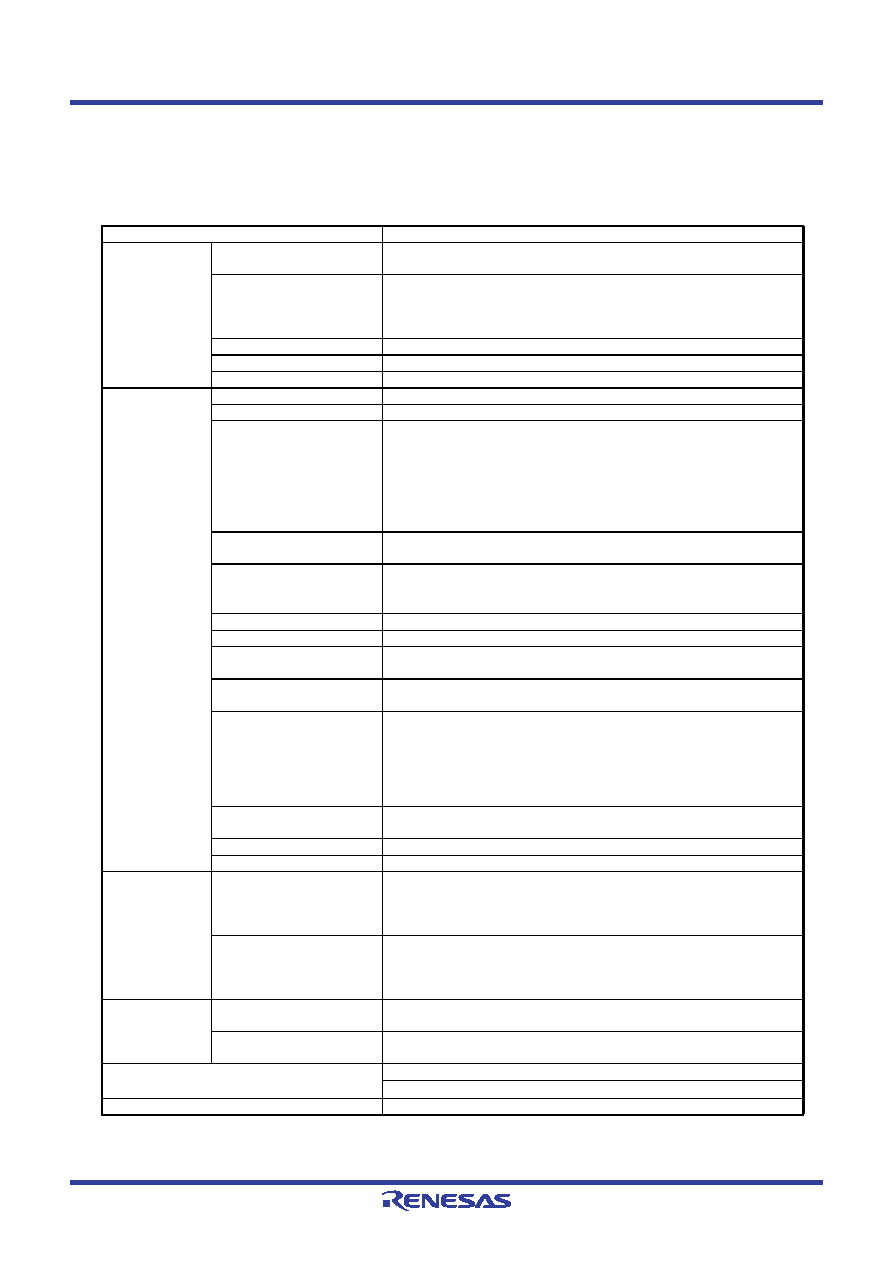
Table 1.1 outlines the Functions and Specifications for R8C/28 Group and Table 1.2 outlines the Functions and
NOTES:
1. I2C bus is a trademark of Koninklijke Philips Electronics N. V.
2. Specify the D, K version if D, K version functions are to be used.
Table 1.1
Functions and Specifications for R8C/28 Group
Item
Specification
CPU
Number of fundamental
instructions
89 instructions
Minimum instruction
execution time
50 ns (f(XIN) = 20 MHz, VCC = 3.0 to 5.5 V) (other than K version)
62.5 ns (f(XIN) = 16 MHz, VCC = 3.0 to 5.5 V) (K version)
100 ns (f(XIN) = 10 MHz, VCC = 2.7 to 5.5 V)
200 ns (f(XIN) = 5 MHz, VCC = 2.2 to 5.5 V) (N, D version)
Operating mode
Single-chip
Address space
1 Mbyte
Memory capacity
Refer to Table 1.3 Product Information for R8C/28 Group
Peripheral
Functions
Ports
I/O ports: 13 pins, Input port: 3 pins
LED drive ports
I/O ports: 8 pins (N, D version)
Timers
Timer RA: 8 bits × 1 channel
Timer RB: 8 bits × 1 channel
(Each timer equipped with 8-bit prescaler)
Timer RC: 16 bits × 1 channel
(Input capture and output compare circuits)
Timer RE: With real-time clock and compare match function
(For J, K version, compare match function only.)
Serial interfaces
1 channel (UART0): Clock synchronous serial I/O, UART
1 channel (UART1): UART
Clock synchronous serial
interface
1 channel
Clock synchronous serial I/O with chip select
LIN module
Hardware LIN: 1 channel (timer RA, UART0)
A/D converter
10-bit A/D converter: 1 circuit, 4 channels
Watchdog timer
15 bits × 1 channel (with prescaler)
Reset start selectable
Interrupts
Internal: 15 sources (N, D version), Internal: 14 sources (J, K version)
External: 4 sources, Software: 4 sources, Priority levels: 7 levels
Clock generation circuits
3 circuits
XIN clock generation circuit (with on-chip feedback resistor)
On-chip oscillator (high speed, low speed)
High-speed on-chip oscillator has a frequency adjustment function
XCIN clock generation circuit (32 kHz) (N, D version)
Real-time clock (timer RE) (N, D version)
Oscillation stop detection
function
XIN clock oscillation stop detection function
Voltage detection circuit
On-chip
Power-on reset circuit
On-chip
Electrical
Characteristics
Supply voltage
VCC = 3.0 to 5.5 V (f(XIN) = 20 MHz) (other than K version)
VCC = 3.0 to 5.5 V (f(XIN) = 16 MHz) (K version)
VCC = 2.7 to 5.5 V (f(XIN) = 10 MHz)
VCC = 2.2 to 5.5 V (f(XIN) = 5 MHz) (N, D version)
Current consumption
(N, D version)
Typ. 10 mA (VCC = 5.0 V, f(XIN) = 20 MHz)
Typ. 6 mA (VCC = 3.0 V, f(XIN) = 10 MHz)
Typ. 2.0
A (VCC = 3.0 V, wait mode (f(XCIN) = 32 kHz)
Typ. 0.7
A (VCC = 3.0 V, stop mode)
Flash Memory
Programming and erasure
voltage
VCC = 2.7 to 5.5 V
Programming and erasure
endurance
100 times
Operating Ambient Temperature
-20 to 85
°C (N version)
-40 to 85
°C (D, J version)(2), -40 to 125°C (K version)(2)
Package
20-pin molded-plastic LSSOP
相关PDF资料 |
PDF描述 |
|---|---|
| R5F21292SNXXXSP | 16-BIT, FLASH, 20 MHz, MICROCONTROLLER, PDSO20 |
| R5F21286KXXXSP | 16-BIT, FLASH, 20 MHz, MICROCONTROLLER, PDSO20 |
| R5F21292SNSP | 16-BIT, FLASH, 20 MHz, MICROCONTROLLER, PDSO20 |
| R5F21294SDXXXSP | 16-BIT, FLASH, 20 MHz, MICROCONTROLLER, PDSO20 |
| R5F21294SDSP | 16-BIT, FLASH, 20 MHz, MICROCONTROLLER, PDSO20 |
相关代理商/技术参数 |
参数描述 |
|---|---|
| R5F21296KSP | 制造商:RENESAS 制造商全称:Renesas Technology Corp 功能描述:SINGLE-CHIP 16-BIT CMOS MCU |
| R5F21296KXXXSP | 制造商:RENESAS 制造商全称:Renesas Technology Corp 功能描述:RENESAS 16-BIT SINGLE-CHIP MCU R8C FAMILY / R8C/2x SERIES |
| R5F212A7SDFA | 制造商:RENESAS 制造商全称:Renesas Technology Corp 功能描述:MCU |
| R5F212A7SDFA#U0 | 制造商:Renesas Electronics Corporation 功能描述:MCU 16-Bit R8C CISC 48KB Flash 2.5V/3.3V/5V 64-Pin LQFP |
| R5F212A7SDFP | 制造商:RENESAS 制造商全称:Renesas Technology Corp 功能描述:MCU |
发布紧急采购,3分钟左右您将得到回复。