- 您现在的位置:买卖IC网 > PDF目录69310 > R5F21388WJFP MICROCONTROLLER, PQFP80 PDF资料下载
参数资料
| 型号: | R5F21388WJFP |
| 元件分类: | 微控制器/微处理器 |
| 英文描述: | MICROCONTROLLER, PQFP80 |
| 封装: | 12 X 12MM, 0.5MM PITCH, PLASTIC, LQFP-80 |
| 文件页数: | 10/70页 |
| 文件大小: | 632K |
| 代理商: | R5F21388WJFP |
第1页第2页第3页第4页第5页第6页第7页第8页第9页当前第10页第11页第12页第13页第14页第15页第16页第17页第18页第19页第20页第21页第22页第23页第24页第25页第26页第27页第28页第29页第30页第31页第32页第33页第34页第35页第36页第37页第38页第39页第40页第41页第42页第43页第44页第45页第46页第47页第48页第49页第50页第51页第52页第53页第54页第55页第56页第57页第58页第59页第60页第61页第62页第63页第64页第65页第66页第67页第68页第69页第70页
R8C/38W Group, R8C/38X Group, R8C/38Y Group, R8C/38Z Group
1. Overview
Under development Preliminary document
Specifications in this document are tentative and subject to change.
REJ03B0317-0010 Rev.0.10
Page 18 of 67
May 31, 2010
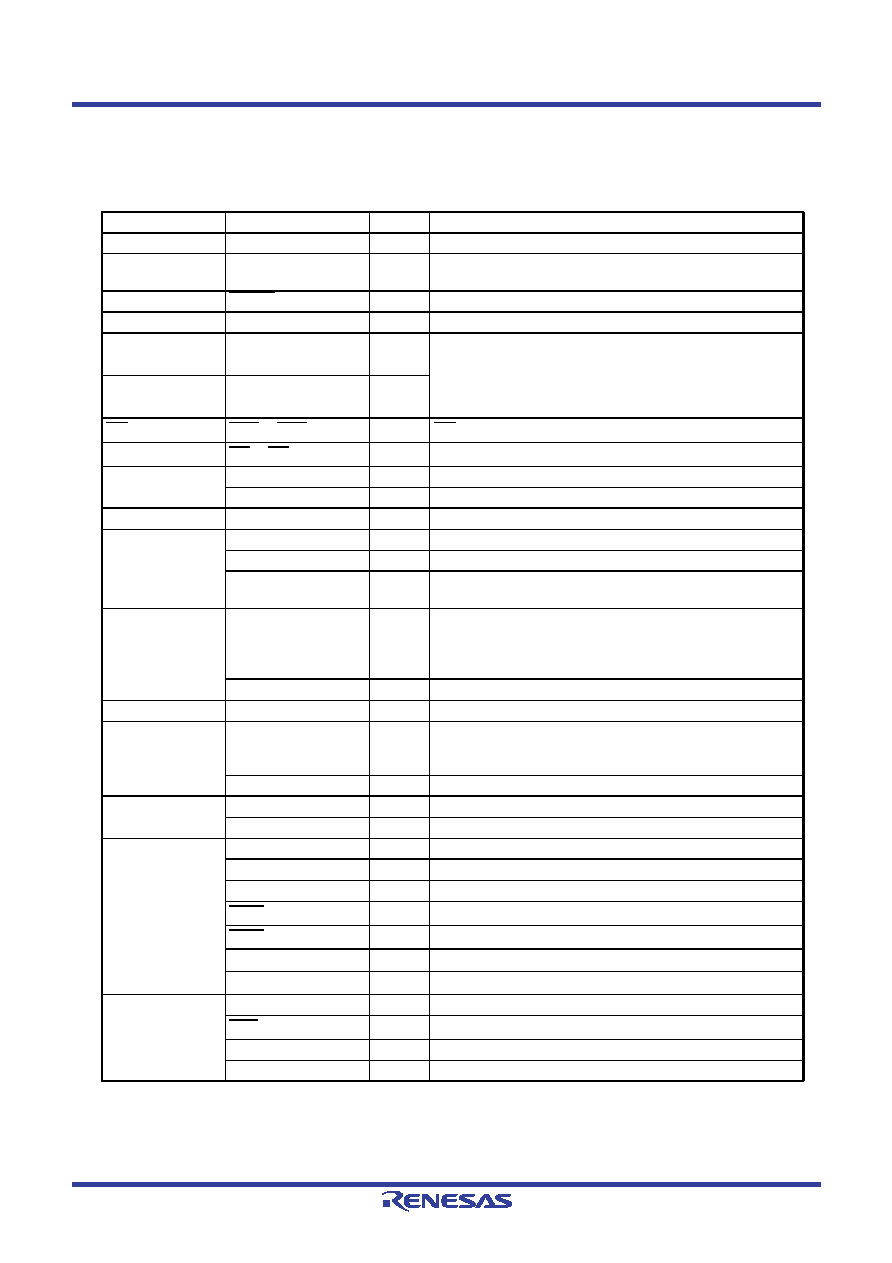
1.5
Pin Functions
I: Input
O: Output
I/O: Input and output
Note:
1. Refer to the oscillator manufacturer for oscillation characteristics.
Table 1.15
Pin Functions (1)
Item
Pin Name
I/O Type
Description
Power supply input VCC, VSS
Apply 2.7 V to 5.5 V to the VCC pin. Apply 0 V to the VSS pin.
Analog power
supply input
AVCC, AVSS
Power supply for the A/D converter.
Connect a capacitor between AVCC and AVSS.
Reset input
RESET
I
Input “L” on this pin resets the MCU.
MODE
I
Connect this pin to VCC via a resistor.
XIN clock input
XIN
I
These pins are provided for XIN clock generation circuit I/O.
Connect a ceramic resonator or a crystal oscillator between
the XIN and XOUT pins (1). To use an external clock, input it
to the XOUT pin and leave the XIN pin open.
XIN clock output
XOUT
I/O
INT interrupt input
INT0 to INT4
IINT interrupt input pins.
Key input interrupt
KI0 to KI3
I
Key input interrupt input pins
Timer RA0
Timer RA1
TRAIO0, TRAIO1
I/O
Timer RA I/O pin
TRAO0, TRAO1
O
Timer RA output pin
Timer RB
TRBO
O
Timer RB output pin
Timer RC
TRCCLK
I
External clock input pin
TRCTRG
I
External trigger input pin
TRCIOA, TRCIOB,
TRCIOC, TRCIOD
I/O
Timer RC I/O pins
Timer RD
TRDIOA0, TRDIOA1,
TRDIOB0, TRDIOB1,
TRDIOC0, TRDIOC1,
TRDIOD0, TRDIOD1
I/O
Timer RD I/O pins
TRDCLK
I
External clock input pin
Timer RE
TREO
O
Divided clock output pin
Timer RF
TRFO00, TRFO10,
TRFO01, TRFO11,
TRFO02, TRFO12
O
Timer RF output pins.
TRFI
I
Timer RF input pin.
Timer RG
TRGIOA, TRGIOB
I/O
Timer RG I/O ports.
TRGCLKA, TRGCLKB
I
External clock input pins.
Serial interface
CLK0, CLK1, CLK2
I/O
Transfer clock I/O pins
RXD0, RXD1, RXD2
I
Serial data input pins
TXD0, TXD1, TXD2
O
Serial data output pins
CTS2
I
Transmission control input pin
RTS2
O
Reception control output pin
SCL2
I/O
I2C mode clock I/O pin
SDA2
I/O
I2C mode data I/O pin
SSU
SSI
I/O
Data I/O pin
SCS
I/O
Chip-select signal I/O pin
SSCK
I/O
Clock I/O pin
SSO
I/O
Data I/O pin
相关PDF资料 |
PDF描述 |
|---|---|
| R5F2138AEJFP | FLASH, 20 MHz, MICROCONTROLLER, PQFP80 |
| R5F2138CGKFP | FLASH, 20 MHz, MICROCONTROLLER, PQFP80 |
| R5F21388HKFP | FLASH, 20 MHz, MICROCONTROLLER, PQFP80 |
| R5F2138AFKFP | FLASH, 20 MHz, MICROCONTROLLER, PQFP80 |
| R5F2138AHJFP | FLASH, 20 MHz, MICROCONTROLLER, PQFP80 |
相关代理商/技术参数 |
参数描述 |
|---|---|
| R5F21388WKFP | 制造商:RENESAS 制造商全称:Renesas Technology Corp 功能描述:RENESAS MCU |
| R5F21388XJFP | 制造商:RENESAS 制造商全称:Renesas Technology Corp 功能描述:RENESAS MCU |
| R5F21388XKFP | 制造商:RENESAS 制造商全称:Renesas Technology Corp 功能描述:RENESAS MCU |
| R5F21388YJFP | 制造商:RENESAS 制造商全称:Renesas Technology Corp 功能描述:RENESAS MCU |
| R5F21388YKFP | 制造商:RENESAS 制造商全称:Renesas Technology Corp 功能描述:RENESAS MCU |
发布紧急采购,3分钟左右您将得到回复。