- 您现在的位置:买卖IC网 > PDF目录69312 > R5F2L3ACCDFA 8-BIT, FLASH, 20 MHz, MICROCONTROLLER, PQFP100 PDF资料下载
参数资料
| 型号: | R5F2L3ACCDFA |
| 元件分类: | 微控制器/微处理器 |
| 英文描述: | 8-BIT, FLASH, 20 MHz, MICROCONTROLLER, PQFP100 |
| 封装: | 14 X 20 MM, 0.65 MM PITCH, PLASTIC, QFP-100 |
| 文件页数: | 19/74页 |
| 文件大小: | 959K |
| 代理商: | R5F2L3ACCDFA |
第1页第2页第3页第4页第5页第6页第7页第8页第9页第10页第11页第12页第13页第14页第15页第16页第17页第18页当前第19页第20页第21页第22页第23页第24页第25页第26页第27页第28页第29页第30页第31页第32页第33页第34页第35页第36页第37页第38页第39页第40页第41页第42页第43页第44页第45页第46页第47页第48页第49页第50页第51页第52页第53页第54页第55页第56页第57页第58页第59页第60页第61页第62页第63页第64页第65页第66页第67页第68页第69页第70页第71页第72页第73页第74页
27
2588F–AVR–06/2013
ATtiny261/461/861
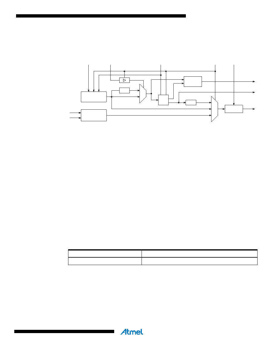
The fast peripheral clock, clk
PCK, can be selected as the clock source for Timer/Counter1 and a
prescaled version of the PLL output, clk
PLL, can be selected as system clock. See Figure 6-3 for
a detailed illustration on the PLL clock system.
Figure 6-3.
PCK Clocking System
The internal PLL is enabled when CKSEL fuse bits are programmed to ‘0001’and the PLLE bit of
PLLCSR is set. The internal oscillator and the PLL are switched off in power down and stand-by
sleep modes.
When the LSM bit of PLLCSR is set, the PLL switches from using the output of the internal 8
MHz oscillator to using the output divided by two. The frequency of the fast peripheral clock is
effectively divided by two, resulting in a clock frequency of 32 MHz. The LSM bit can not be set if
PLL
CLK is used as a system clock.
Since the PLL is locked to the output of the internal 8 MHz oscillator, adjusting the oscillator fre-
quency via the OSCCAL register also changes the frequency of the fast peripheral clock. It is
possible to adjust the frequency of the internal oscillator to well above 8 MHz but the fast periph-
eral clock will saturate and remain oscillating at about 85 MHz. In this case the PLL is no longer
locked to the internal oscillator clock signal. Therefore, in order to keep the PLL in the correct
operating range, it is recommended to program the OSCCAL registers such that the oscillator
frequency does not exceed 8 MHz.
The PLOCK bit in PLLCSR is set when PLL is locked.
Programming CKSEL fuse bits to ‘0001’, the PLL output divided by four will be used as a system
clock, as shown in Table 6-4.
Table 6-4.
PLLCK Operating Modes
CKSEL3:0
Nominal Frequency
0001
16 MHz
1/2
8 MHz
LSM
8 MHz
OSCILLATOR
PLL
8x
CKSEL3:0
PLLE
OSCCAL
4 MHz
1/4
LOCK
DETECTOR
PRESCALER
CLKPS3:0
clkPLL
PLOCK
clkPCK
OSCILLATORS
XTAL1
XTAL2
64 / 32 MHz
8 MHz
16 MHz
相关PDF资料 |
PDF描述 |
|---|---|
| R5F2L38CCNFA | 8-BIT, FLASH, 20 MHz, MICROCONTROLLER, PQFP80 |
| R5F2L388CNFP | 8-BIT, FLASH, 20 MHz, MICROCONTROLLER, PQFP80 |
| R5F2L3A8CNFA | 8-BIT, FLASH, 20 MHz, MICROCONTROLLER, PQFP100 |
| R5F2L36CCNFP | 8-BIT, FLASH, 20 MHz, MICROCONTROLLER, PQFP64 |
| R5F2L367CDFA | 8-BIT, FLASH, 20 MHz, MICROCONTROLLER, PQFP64 |
相关代理商/技术参数 |
参数描述 |
|---|---|
| R5F2L3ACCDFA#U0 | 功能描述:MCU 128KB ROM 10KB RAM 100LQFP RoHS:是 类别:集成电路 (IC) >> 嵌入式 - 微控制器, 系列:R8C/Lx/3AC 标准包装:250 系列:80C 核心处理器:8051 芯体尺寸:8-位 速度:16MHz 连通性:EBI/EMI,I²C,UART/USART 外围设备:POR,PWM,WDT 输入/输出数:40 程序存储器容量:- 程序存储器类型:ROMless EEPROM 大小:- RAM 容量:256 x 8 电压 - 电源 (Vcc/Vdd):4.5 V ~ 5.5 V 数据转换器:A/D 8x10b 振荡器型:内部 工作温度:-40°C ~ 85°C 封装/外壳:68-LCC(J 形引线) 包装:带卷 (TR) |
| R5F2L3ACCDFP#V0 | 功能描述:MCU 128KB ROM 10KB RAM 100-LQFP RoHS:是 类别:集成电路 (IC) >> 嵌入式 - 微控制器, 系列:R8C/Lx/3AC 标准包装:250 系列:80C 核心处理器:8051 芯体尺寸:8-位 速度:16MHz 连通性:EBI/EMI,I²C,UART/USART 外围设备:POR,PWM,WDT 输入/输出数:40 程序存储器容量:- 程序存储器类型:ROMless EEPROM 大小:- RAM 容量:256 x 8 电压 - 电源 (Vcc/Vdd):4.5 V ~ 5.5 V 数据转换器:A/D 8x10b 振荡器型:内部 工作温度:-40°C ~ 85°C 封装/外壳:68-LCC(J 形引线) 包装:带卷 (TR) |
| R5F2L3ACCNFA#U0 | 功能描述:MCU 128KB ROM 10KB RAM 100-LQFP RoHS:是 类别:集成电路 (IC) >> 嵌入式 - 微控制器, 系列:R8C/Lx/3AC 标准包装:250 系列:80C 核心处理器:8051 芯体尺寸:8-位 速度:16MHz 连通性:EBI/EMI,I²C,UART/USART 外围设备:POR,PWM,WDT 输入/输出数:40 程序存储器容量:- 程序存储器类型:ROMless EEPROM 大小:- RAM 容量:256 x 8 电压 - 电源 (Vcc/Vdd):4.5 V ~ 5.5 V 数据转换器:A/D 8x10b 振荡器型:内部 工作温度:-40°C ~ 85°C 封装/外壳:68-LCC(J 形引线) 包装:带卷 (TR) |
| R5F2L3ACCNFP#30 | 制造商:Renesas Electronics Corporation 功能描述:IC MCU 16BIT 128KB FLASH 100LQFP |
| R5F2L3ACCNFP#U1 | 制造商:Renesas Electronics Corporation 功能描述: |
发布紧急采购,3分钟左右您将得到回复。