- 您现在的位置:买卖IC网 > PDF目录11673 > R5F5630EDDFB#V0 (Renesas Electronics America)MCU RX630 2MB FLASH 144-LQFP PDF资料下载
参数资料
| 型号: | R5F5630EDDFB#V0 |
| 厂商: | Renesas Electronics America |
| 文件页数: | 19/165页 |
| 文件大小: | 0K |
| 描述: | MCU RX630 2MB FLASH 144-LQFP |
| 产品培训模块: | RX Compare Match Timer RX DMAC |
| 标准包装: | 1 |
| 系列: | RX600 |
| 核心处理器: | RX |
| 芯体尺寸: | 32-位 |
| 速度: | 100MHz |
| 连通性: | CAN,EBI/EMI,I²C,LIN,SCI,SPI,USB |
| 外围设备: | DMA,LVD,POR,PWM,WDT |
| 输入/输出数: | 117 |
| 程序存储器容量: | 2MB(2M x 8) |
| 程序存储器类型: | 闪存 |
| RAM 容量: | 128K x 8 |
| 电压 - 电源 (Vcc/Vdd): | 2.7 V ~ 3.6 V |
| 数据转换器: | A/D 8x10b,21x12b,D/A 2x10b |
| 振荡器型: | 内部 |
| 工作温度: | -40°C ~ 85°C |
| 封装/外壳: | 144-LQFP |
| 包装: | 托盘 |
第1页第2页第3页第4页第5页第6页第7页第8页第9页第10页第11页第12页第13页第14页第15页第16页第17页第18页当前第19页第20页第21页第22页第23页第24页第25页第26页第27页第28页第29页第30页第31页第32页第33页第34页第35页第36页第37页第38页第39页第40页第41页第42页第43页第44页第45页第46页第47页第48页第49页第50页第51页第52页第53页第54页第55页第56页第57页第58页第59页第60页第61页第62页第63页第64页第65页第66页第67页第68页第69页第70页第71页第72页第73页第74页第75页第76页第77页第78页第79页第80页第81页第82页第83页第84页第85页第86页第87页第88页第89页第90页第91页第92页第93页第94页第95页第96页第97页第98页第99页第100页第101页第102页第103页第104页第105页第106页第107页第108页第109页第110页第111页第112页第113页第114页第115页第116页第117页第118页第119页第120页第121页第122页第123页第124页第125页第126页第127页第128页第129页第130页第131页第132页第133页第134页第135页第136页第137页第138页第139页第140页第141页第142页第143页第144页第145页第146页第147页第148页第149页第150页第151页第152页第153页第154页第155页第156页第157页第158页第159页第160页第161页第162页第163页第164页第165页
R01DS0060EJ0100 Rev.1.00
Page 115 of 168
Sep 13, 2011
RX630 Group
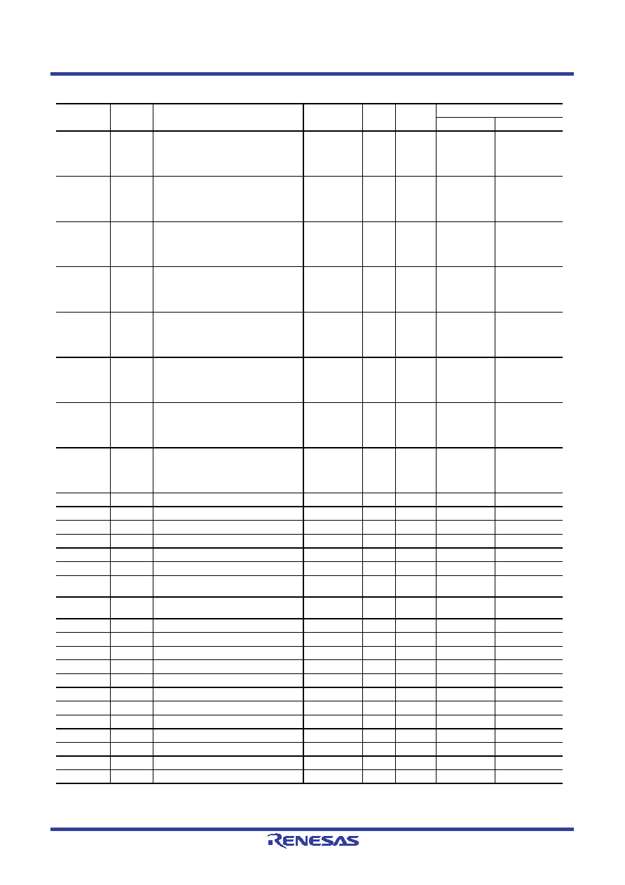
4. I/O Registers
○: Available, ×: Not available
000A 0098h
USB0
Pipe 3 transaction counter enable register
PIPE3TRE
16
9 PCLKB or
more
Rounded up to the
nearest integer
greater than 1 + 9/
(frequency ratio of
ICLK/PCLKB)*8
000A 009Ah
USB0
Pipe 3 transaction counter register
PIPE3TRN
16
9 PCLKB or
more
Rounded up to the
nearest integer
greater than 1 + 9/
(frequency ratio of
ICLK/PCLKB)*8
000A 009Ch
USB0
Pipe 4 transaction counter enable register
PIPE4TRE
16
9 PCLKB or
more
Rounded up to the
nearest integer
greater than 1 + 9/
(frequency ratio of
ICLK/PCLKB)*8
000A 009Eh
USB0
Pipe 4 transaction counter register
PIPE4TRN
16
9 PCLKB or
more
Rounded up to the
nearest integer
greater than 1 + 9/
(frequency ratio of
ICLK/PCLKB)*8
000A 00A0h
USB0
Pipe 5 transaction counter enable register
PIPE5TRE
16
9 PCLKB or
more
Rounded up to the
nearest integer
greater than 1 + 9/
(frequency ratio of
ICLK/PCLKB)*8
000A 00A2h
USB0
Pipe 5 transaction counter register
PIPE5TRN
16
9 PCLKB or
more
Rounded up to the
nearest integer
greater than 1 + 9/
(frequency ratio of
ICLK/PCLKB)*8
000A 0400h
USB0
Deep standby USB transceiver control/pin
monitor register
DPUSR0R
32
9 PCLKB or
more
Rounded up to the
nearest integer
greater than 1 + 9/
(frequency ratio of
ICLK/PCLKB)*8
000A 0404h
USB0
Deep standby USB suspend/resume interrupt
register
DPUSR1R
32
9 PCLKB or
more
Rounded up to the
nearest integer
greater than 1 + 9/
(frequency ratio of
ICLK/PCLKB)*8
007F C402h
FLASH
Flash mode register
FMODR
8
2, 3 FCLK
2, 3 ICLK
007F C410h
FLASH
Flash access status register
FASTAT
8
2, 3 FCLK
2, 3 ICLK
007F C411h
FLASH
Flash access error interrupt enable register
FAEINT
8
2, 3 FCLK
2, 3 ICLK
007F C412h
FLASH
Flash ready interrupt enable register
FRDYIE
8
2, 3 FCLK
2, 3 ICLK
007F C440h
FLASH
E2 data flash read enable register 0
DFLRE0
16
2, 3 FCLK
2, 3 ICLK
007F C442h
FLASH
E2 data flash read enable register 1
DFLRE1
16
2, 3 FCLK
2, 3 ICLK
007F C450h
FLASH
E2 data flash programming/erasure enable
register 0
DFLWE0
16
2, 3 FCLK
2, 3 ICLK
007F C452h
FLASH
E2 data flash programming/erasure enable
register 1
DFLWE1
16
2, 3 FCLK
2, 3 ICLK
007F C454h
FLASH
FCU RAM enable register
FCURAME
16
2, 3 FCLK
2, 3 ICLK
007F FFB0h
FLASH
Flash status register 0
FSTATR0
8
2, 3 FCLK
2, 3 ICLK
007F FFB1h
FLASH
Flash status register 1
FSTATR1
8
2, 3 FCLK
2, 3 ICLK
007F FFB2h
FLASH
Flash P/E mode entry register
FENTRYR
16
2, 3 FCLK
2, 3 ICLK
007F FFB4h
FLASH
Flash protection register
FPROTR
16
2, 3 FCLK
2, 3 ICLK
007F FFB6h
FLASH
Flash reset register
FRESETR
16
2, 3 FCLK
2, 3 ICLK
007F FFBAh
FLASH
FCU command register
FCMDR
16
2, 3 FCLK
2, 3 ICLK
007F FFC8h
FLASH
FCU processing switching register
FCPSR
16
2, 3 FCLK
2, 3 ICLK
007F FFCAh
FLASH
E2 data flash blank check control register
DFLBCCNT
16
2, 3 FCLK
2, 3 ICLK
007F FFCCh
FLASH
Flash P/E status register
FPESTAT
16
2, 3 FCLK
2, 3 ICLK
007F FFCEh
FLASH
E2 data flash blank check status register
DFLBCSTAT
16
2, 3 FCLK
2, 3 ICLK
007F FFE8h
FLASH
Peripheral clock notification register
PCKAR
16
2, 3 FCLK
2, 3 ICLK
Note 1.
When the same output trigger is specified for pulse output groups 2 and 3 by the PPG0.PCR setting, the PPG0.NDRH address is 000881ECh. When different output
triggers are specified, the PPG0.NDRH addresses for pulse output groups 2 and 3 are 000881EEh and 000881ECh, respectively.
Table 4.1
List of I/O Registers (Address Order) (39/39)
Address
Module
Symbol
Register Name
Register Symbol
Number
of Bits
Access
Size
Number of Access States
ICLK
PCLK
ICLK
PCLK
相关PDF资料 |
PDF描述 |
|---|---|
| R5F56108VDFP#V0 | MCU 32BIT FLASH 2M ROM 144LQFP |
| MS27484E16F55S | CONN PLUG 55POS STRAIGHT W/SCKT |
| MS3101F28-16S | CONN RCPT 20POS FREE HNG W/SCKT |
| VE-J33-IY-F1 | CONVERTER MOD DC/DC 24V 50W |
| VE-J32-IZ-B1 | CONVERTER MOD DC/DC 15V 25W |
相关代理商/技术参数 |
参数描述 |
|---|---|
| R5F5630EDDFC | 制造商:Renesas Electronics Corporation 功能描述:MCU 32BIT RX630 176LQFP 制造商:Renesas Electronics Corporation 功能描述:MCU, 32BIT, RX630, 176LQFP 制造商:Renesas Electronics Corporation 功能描述:MCU, 32BIT, RX630, 176LQFP; Controller Family/Series:RX600; Core Size:32bit; No. of I/O's:148; Supply Voltage Min:2.7V; Supply Voltage Max:3.6V; Digital IC Case Style:LQFP; No. of Pins:176; Program Memory Size:2MB; RAM Memory ;RoHS Compliant: Yes |
| R5F5630EDDFC#V0 | 功能描述:MCU RX630 2MB FLASH 176-LQFP RoHS:是 类别:集成电路 (IC) >> 嵌入式 - 微控制器, 系列:RX600 标准包装:96 系列:PIC® 16F 核心处理器:PIC 芯体尺寸:8-位 速度:20MHz 连通性:I²C,SPI 外围设备:欠压检测/复位,POR,PWM,WDT 输入/输出数:11 程序存储器容量:3.5KB(2K x 14) 程序存储器类型:闪存 EEPROM 大小:- RAM 容量:128 x 8 电压 - 电源 (Vcc/Vdd):2.3 V ~ 5.5 V 数据转换器:A/D 8x10b 振荡器型:内部 工作温度:-40°C ~ 125°C 封装/外壳:14-TSSOP(0.173",4.40mm 宽) 包装:管件 |
| R5F5630EDDFP | 制造商:RENESAS 制造商全称:Renesas Technology Corp 功能描述:Renesas MCUs |
| R5F5630EDDFP#V0 | 功能描述:MCU RX630 2MB FLASH 100-LQFP RoHS:是 类别:集成电路 (IC) >> 嵌入式 - 微控制器, 系列:RX600 标准包装:96 系列:PIC® 16F 核心处理器:PIC 芯体尺寸:8-位 速度:20MHz 连通性:I²C,SPI 外围设备:欠压检测/复位,POR,PWM,WDT 输入/输出数:11 程序存储器容量:3.5KB(2K x 14) 程序存储器类型:闪存 EEPROM 大小:- RAM 容量:128 x 8 电压 - 电源 (Vcc/Vdd):2.3 V ~ 5.5 V 数据转换器:A/D 8x10b 振荡器型:内部 工作温度:-40°C ~ 125°C 封装/外壳:14-TSSOP(0.173",4.40mm 宽) 包装:管件 |
| R5F5630EDDFPV0 | 制造商:Renesas Electronics Corporation 功能描述:32bitMCU, RX,2048K ROM,128K RAM,LFQFP100 |
发布紧急采购,3分钟左右您将得到回复。