- 您现在的位置:买卖IC网 > PDF目录11673 > R5F5630EDDFC#V0 (Renesas Electronics America)MCU RX630 2MB FLASH 176-LQFP PDF资料下载
参数资料
| 型号: | R5F5630EDDFC#V0 |
| 厂商: | Renesas Electronics America |
| 文件页数: | 25/165页 |
| 文件大小: | 0K |
| 描述: | MCU RX630 2MB FLASH 176-LQFP |
| 产品培训模块: | RX Compare Match Timer RX DMAC |
| 标准包装: | 1 |
| 系列: | RX600 |
| 核心处理器: | RX |
| 芯体尺寸: | 32-位 |
| 速度: | 100MHz |
| 连通性: | CAN,EBI/EMI,I²C,LIN,SCI,SPI,USB |
| 外围设备: | DMA,LVD,POR,PWM,WDT |
| 输入/输出数: | 148 |
| 程序存储器容量: | 2MB(2M x 8) |
| 程序存储器类型: | 闪存 |
| RAM 容量: | 128K x 8 |
| 电压 - 电源 (Vcc/Vdd): | 2.7 V ~ 3.6 V |
| 数据转换器: | A/D 8x10b,21x12b,D/A 2x10b |
| 振荡器型: | 内部 |
| 工作温度: | -40°C ~ 85°C |
| 封装/外壳: | 176-LQFP |
| 包装: | 托盘 |
第1页第2页第3页第4页第5页第6页第7页第8页第9页第10页第11页第12页第13页第14页第15页第16页第17页第18页第19页第20页第21页第22页第23页第24页当前第25页第26页第27页第28页第29页第30页第31页第32页第33页第34页第35页第36页第37页第38页第39页第40页第41页第42页第43页第44页第45页第46页第47页第48页第49页第50页第51页第52页第53页第54页第55页第56页第57页第58页第59页第60页第61页第62页第63页第64页第65页第66页第67页第68页第69页第70页第71页第72页第73页第74页第75页第76页第77页第78页第79页第80页第81页第82页第83页第84页第85页第86页第87页第88页第89页第90页第91页第92页第93页第94页第95页第96页第97页第98页第99页第100页第101页第102页第103页第104页第105页第106页第107页第108页第109页第110页第111页第112页第113页第114页第115页第116页第117页第118页第119页第120页第121页第122页第123页第124页第125页第126页第127页第128页第129页第130页第131页第132页第133页第134页第135页第136页第137页第138页第139页第140页第141页第142页第143页第144页第145页第146页第147页第148页第149页第150页第151页第152页第153页第154页第155页第156页第157页第158页第159页第160页第161页第162页第163页第164页第165页
R01DS0060EJ0100 Rev.1.00
Page 120 of 168
Sep 13, 2011
RX630 Group
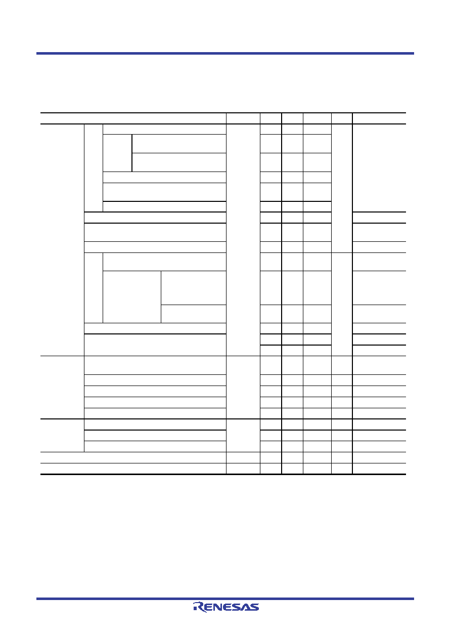
5. Electrical Characteristics
Note 1. Supply current values are with all output pins unloaded and all input pull-up MOSs in the off state.
Note 2. Measured with clocks supplied to the peripheral functions. This does not include the BGO operation.
Note 3. ICC depends on f (ICLK) as follows. (ICLK:PCLK:BCLK:BCLK pin = 8:4:4:2)
ICC Max. = 0.87 × f + 13 (max. operation in high-speed operating mode)
ICC Typ. = 0.35 × f + 5 (normal operation in high-speed operating mode)
ICC Typ. = 1.0 × f + 3 (low-speed operating mode 1)
ICC Max. = 0.48 × f + 12 (sleep mode)
Note 4. This does not include the BGO operation.
Note 5. This is the increase for programming or erasure of the ROM or flash memory for data storage during program execution.
Note 6. Supply of the clock signal to peripherals is stopped in this state. This does not include the BGO operation.
Note 7. The reference power supply current is included in the power supply current value for 10-bit A/D conversion and D/A conversion.
Note 8. When VBATT is used
Table 5.4
DC Characteristics (3)
Conditions: VCC = AVCC0 = VCC_USB = VBATT = 2.7 to 3.6 V, VREFH/VREFH0 = 2.7 V to AVCC0,
VSS = AVSS0 = VREFL/VREFL0 = VSS_USB = 0 V, Ta = Topr
Item
Symbol
Min.
Typ.
Max.
Unit
Test Conditions
Supply
current*1
High
-speed
oper
ating
mode
Max.*2
ICC*3
—
100
mA
ICLK = 100 MHz
PCLKB = 50 MHz
FCLK = 50 MHz
BCLK = 50 MHz
Normal
Peripheral function: clock signal
supplied*4
—52
—
Peripheral function: clock signal
—40
—
Sleep mode
—
25
60
All-module-clock-stop mode (reference
value)
—20
30
Increased by BGO operation*5
—15
—
Low-speed operating mode 1*6
—4
—
ICLK = 1 MHz
Low-speed operating mode 2
—
1
—
ICLK = 32.768
kHz
Software standby mode
—
0.2
6
Deep
sof
twar
e
st
and
by
mode
Power supplied to on-chip RAM and USB
resume detecting unit
—
22
200
A
Power not supplied
to on-chip RAM
and USB resume
detecting unit
Power-on reset circuit
and low-power
consumption function
disabled
—21
60
Power-on reset circuit
and low-power
—6.2
28
Increased by RTC operation
—
3
—
RTC operation when VCC is off
—
1.7
—
VBATT = 2.3 V
—
3.3
—
VBATT = 3.3 V
Analog power
supply
current*7
During 12-bit A/D conversion (including
temperature sensor)
AICC
—
2.3
3.2
mA
During 10-bit A/D conversion
—
1.0
1.65
mA
During D/A conversion (per unit)
—
0.7
1.0
mA
Waiting for A/D, D/A conversion (all units)
—
25
35
A
A/D, D/A converter in standby mode (all units)
—
0.1
4.0
A
Reference
power supply
current
During 12-bit A/D conversion
IREFH
—
0.6
0.7
mA
Waiting for 12-bit A/D conversion (per unit)
—
0.5
0.6
mA
12-bit A/D converter in standby mode (per unit)
—
0.1
2.0
A
VCC rising gradient
SrVCC
8.4
—
20000
s/V
VCC falling gradient*8
SfVCC
8.4
—
s/V
相关PDF资料 |
PDF描述 |
|---|---|
| D38999/20JE6PA | CONN RCPT 6POS WALL MNT W/PINS |
| MS27473T24B35SC | CONN PLUG 128POS STRAIGHT W/SCKT |
| D38999/26FE6SN | CONN PLUG 6POS STRAIGHT W/SCKT |
| GTC06AF-22-14S | CONN PLUG 19POS STRAIGHT W/SCKT |
| VE-J3F-IY-F1 | CONVERTER MOD DC/DC 72V 50W |
相关代理商/技术参数 |
参数描述 |
|---|---|
| R5F5630EDDFP | 制造商:RENESAS 制造商全称:Renesas Technology Corp 功能描述:Renesas MCUs |
| R5F5630EDDFP#V0 | 功能描述:MCU RX630 2MB FLASH 100-LQFP RoHS:是 类别:集成电路 (IC) >> 嵌入式 - 微控制器, 系列:RX600 标准包装:96 系列:PIC® 16F 核心处理器:PIC 芯体尺寸:8-位 速度:20MHz 连通性:I²C,SPI 外围设备:欠压检测/复位,POR,PWM,WDT 输入/输出数:11 程序存储器容量:3.5KB(2K x 14) 程序存储器类型:闪存 EEPROM 大小:- RAM 容量:128 x 8 电压 - 电源 (Vcc/Vdd):2.3 V ~ 5.5 V 数据转换器:A/D 8x10b 振荡器型:内部 工作温度:-40°C ~ 125°C 封装/外壳:14-TSSOP(0.173",4.40mm 宽) 包装:管件 |
| R5F5630EDDFPV0 | 制造商:Renesas Electronics Corporation 功能描述:32bitMCU, RX,2048K ROM,128K RAM,LFQFP100 |
| R5F5630EDDLC | 制造商:RENESAS 制造商全称:Renesas Technology Corp 功能描述:Renesas MCUs |
| R5F5630EDDLK | 制造商:RENESAS 制造商全称:Renesas Technology Corp 功能描述:Renesas MCUs |
发布紧急采购,3分钟左右您将得到回复。