- 您现在的位置:买卖IC网 > PDF目录69314 > R5F64114NFB 32-BIT, FLASH, 50 MHz, MICROCONTROLLER, PQFP100 PDF资料下载
参数资料
| 型号: | R5F64114NFB |
| 元件分类: | 微控制器/微处理器 |
| 英文描述: | 32-BIT, FLASH, 50 MHz, MICROCONTROLLER, PQFP100 |
| 封装: | 14 X 14 MM, 0.50 MM PITCH, PLASTIC, LQFP-100 |
| 文件页数: | 26/84页 |
| 文件大小: | 1206K |
| 代理商: | R5F64114NFB |
第1页第2页第3页第4页第5页第6页第7页第8页第9页第10页第11页第12页第13页第14页第15页第16页第17页第18页第19页第20页第21页第22页第23页第24页第25页当前第26页第27页第28页第29页第30页第31页第32页第33页第34页第35页第36页第37页第38页第39页第40页第41页第42页第43页第44页第45页第46页第47页第48页第49页第50页第51页第52页第53页第54页第55页第56页第57页第58页第59页第60页第61页第62页第63页第64页第65页第66页第67页第68页第69页第70页第71页第72页第73页第74页第75页第76页第77页第78页第79页第80页第81页第82页第83页第84页
REJ03B0227-0110 Rev.1.10 Sep 17, 2009
Page 24 of 99
R32C/111 Group
1. Overview
1.5
Pin Definitions and Functions
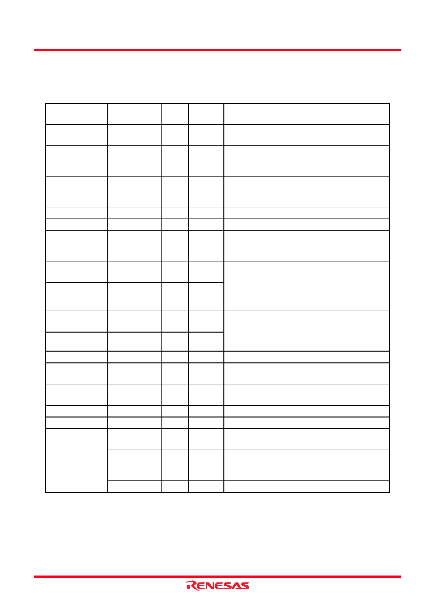
Table 1.15 to Table 1.21 show the pin definitions and functions.
Table 1.15
Pin Definitions and Functions for the 100-pin Package (1/4)
Function
Symbol
I/O
Power
Supply
Description
Power supply
VCC1, VCC2,
VSS
I—
Applicable as follows: VCC1 and VCC2 = 3.0 to
5.5 V (VCC1
≥ VCC2), VSS = 0 V
Connecting pins
for decoupling
capacitor
VDC0, VDC1
——
A decoupling capacitor for internal voltage should
be connected between VDC0 and VDC1
Analog power
supply
AVCC, AVSS
I
VCC1
Power supply for the A/D converter. AVCC and
AVSS should be connected to VCC1 and VSS,
respectively
Reset input
RESET
I
VCC1
The MCU is reset when this pin is driven low
CNVSS
I
VCC1
This pin should be connected to VSS via a resistor
Debug port
NSD
I/O
VCC1
This pin is to communicate with a debugger. It
should be connected to VCC1 via a resistor of 1 to
4.7 k
Main clock input
XIN
I
VCC1
Input/output for the main clock oscillator. A crystal,
or a ceramic resonator should be connected
between pins XIN and XOUT. An external clock
should be input at the XIN while leaving the XOUT
open
Main clock output XOUT
O
VCC1
Sub clock input
XCIN
I
VCC1
Input/output for the sub clock oscillator. A crystal
oscillator should be connected between pins XCIN
and XCOUT. An external clock should be input at
the XCIN while leaving the XCOUT open
Sub clock output
XCOUT
O
VCC1
BCLK output
BCLK
O
VCC2
BCLK output
Clock output
CLKOUT
O
VCC2
Output of the clock with the same frequency as fC,
f8, or f32
External interrupt
input
INT0 to INT5
I
VCC1
VCC2
Input for external interrupts
NMI input
P8_5/
NMI
I
VCC1
Input for NMI
Key input interrupt
KI0 to KI3
I
VCC1
Input for the key input interrupt
Bus control pins
D0 to D7
I/O
VCC2
Input/output of data (D0 to D7) while accessing an
external memory space with a separate bus
D8 to D15
I/O
VCC2
Input/output of data (D8 to D15) while accessing
an external memory space with 16-bit separate
bus
A0 to A23
O
VCC2
Output of address bits A0 to A23
相关PDF资料 |
PDF描述 |
|---|---|
| R5F64112DFB | 32-BIT, FLASH, 50 MHz, MICROCONTROLLER, PQFP100 |
| R5F64165PFD | 64-BIT, FLASH, MICROCONTROLLER, PQFP144 |
| R5F64168HNFB | 64-BIT, FLASH, MICROCONTROLLER, PQFP100 |
| R5F64168HDFB | 64-BIT, FLASH, MICROCONTROLLER, PQFP100 |
| R5F64168HPFB | 64-BIT, FLASH, MICROCONTROLLER, PQFP100 |
相关代理商/技术参数 |
参数描述 |
|---|---|
| R5F64115DFB | 制造商:RENESAS 制造商全称:Renesas Technology Corp 功能描述:RENESAS MCU |
| R5F64115DFB#U0 | 功能描述:MCU 384KB ROM 40KB RAM 100-LQFP RoHS:是 类别:集成电路 (IC) >> 嵌入式 - 微控制器, 系列:M16C/R32C/100/111 产品培训模块:CAN Basics Part-1 CAN Basics Part-2 Electromagnetic Noise Reduction Techniques Part 1 M16C Product Overview Part 1 M16C Product Overview Part 2 标准包装:1 系列:M16C™ M32C/80/87 核心处理器:M32C/80 芯体尺寸:16/32-位 速度:32MHz 连通性:EBI/EMI,I²C,IEBus,IrDA,SIO,UART/USART 外围设备:DMA,POR,PWM,WDT 输入/输出数:121 程序存储器容量:384KB(384K x 8) 程序存储器类型:闪存 EEPROM 大小:- RAM 容量:24K x 8 电压 - 电源 (Vcc/Vdd):3 V ~ 5.5 V 数据转换器:A/D 34x10b,D/A 2x8b 振荡器型:内部 工作温度:-20°C ~ 85°C 封装/外壳:144-LQFP 包装:托盘 产品目录页面:749 (CN2011-ZH PDF) 配用:R0K330879S001BE-ND - KIT DEV RSK M32C/87 |
| R5F64115NFB | 制造商:RENESAS 制造商全称:Renesas Technology Corp 功能描述:RENESAS MCU |
| R5F64116DFB | 制造商:RENESAS 制造商全称:Renesas Technology Corp 功能描述:RENESAS MCU |
| R5F64116DFB#U0 | 制造商:Renesas Electronics Corporation 功能描述:MCU 16-Bit R8C CISC 512KB Flash 3.3V/5V 100-Pin LQFP Tray 制造商:Renesas Electronics Corporation 功能描述:MCU 3/5V 512K I-TEMP PB-FREE 100-LQFP - Trays 制造商:Renesas Electronics Corporation 功能描述:MCU 16BIT 512KB FLASH 100LFQFP |
发布紧急采购,3分钟左右您将得到回复。