- 您现在的位置:买卖IC网 > PDF目录225025 > RC1585M15 (FAIRCHILD SEMICONDUCTOR CORP) 1.5 V FIXED POSITIVE LDO REGULATOR, 1.3 V DROPOUT, PSSO3 PDF资料下载
参数资料
| 型号: | RC1585M15 |
| 厂商: | FAIRCHILD SEMICONDUCTOR CORP |
| 元件分类: | 固定正电压单路输出LDO稳压器 |
| 英文描述: | 1.5 V FIXED POSITIVE LDO REGULATOR, 1.3 V DROPOUT, PSSO3 |
| 封装: | PLASTIC, TO-263, 3 PIN |
| 文件页数: | 12/15页 |
| 文件大小: | 181K |
| 代理商: | RC1585M15 |
RC1585
PRODUCT SPECIFICATION
6
REV. 1.1.2
Applications Information
General
The RC1585 and RC1585-1.5 are three-terminal regulators
optimized for GTL+ VTT termination and logic applica-
tions. These devices are short-circuit protected and offer
thermal shutdown to turn off the regulator when the junction
temperature exceeds about 150°C. The RC1585 series pro-
vides low dropout voltage and fast transient response. Fre-
quency compensation uses capacitors with low ESR while
still maintaining stability. This is critical in addressing the
needs of low voltage high speed microprocessor buses like
GTL+.
Stability
The RC1585 series requires an output capacitor as a part of
the frequency compensation. It is recommended to use a
22F solid tantalum or a 100 F aluminum electrolytic on
the output to ensure stability. The frequency compensation of
these devices optimizes the frequency response with low
ESR capacitors. In general, it is suggested to use capacitors
with an ESR of <300m
. It is also recommended to use
bypass capacitors such as a 22F tantalum or a 100F alumi-
num on the adjust pin of the RC1585 for low ripple and fast
transient response. When these bypassing capacitors are not
used at the adjust pin, larger values of output capacitors pro-
vide equally good results.
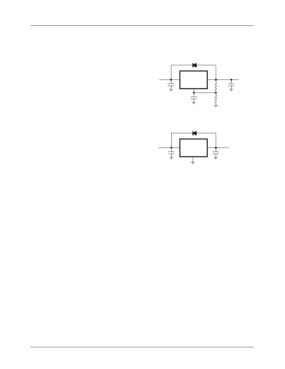
Protection Diodes
In normal operation, the RC1585 series does not require any
protection diodes. For the RC1585, internal resistors limit
internal current paths on the adjust pin. Therefore, even with
bypass capacitors on the adjust pin, no protection diode is
needed to ensure device safety under short-circuit condi-
tions.
A protection diode between the input and output pins is
usually not needed. An internal diode between the input and
the output pins on the RC1585 series can handle micro-
second surge currents of 50A to 100A. Even with large value
output capacitors it is difcult to obtain those values of surge
currents in normal operation. Only with large values of
output capacitance, such as 1000F to 5000F, and with the
input pin instantaneously shorted to ground can damage
occur. A crowbar circuit at the input can generate those
levels of current; a diode from output to input is then recom-
mended, as shown in Figure 10. Usually, normal power sup-
ply cycling or system “hot plugging and unplugging” will
not generate current large enough to do any damage.
The adjust pin can be driven on a transient basis ±7V with
respect to the output, without any device degradation. As
with any IC regulator, exceeding the maximum input-to-
output voltage differential causes the internal transistors to
break down and none of the protection circuitry is then
functional.
Figure 10. Optional Protection
Ripple Rejection
In applications that require improved ripple rejection, a
bypass capacitor from the adjust pin of the RC1585 to
ground reduces the output ripple by the ratio of VOUT/1.25V.
The impedance of the adjust pin capacitor at the ripple fre-
quency should be less than the value of R1 (typically in the
range of 100
to 120) in the feedback divider network in
Figure 10. Therefore, the value of the required adjust pin
capacitor is a function of the input ripple frequency. For
example, if R1 equals 100
and the ripple frequency equals
120Hz, the adjust pin capacitor should be 22F. At 10kHz,
only 0.22F is needed.
Output Voltage
The RC1585 regulator develops a 1.25V reference voltage
between the output pin and the adjust pin (see Figure 11).
Placing a resistor R1 between these two terminals causes a
constant current to ow through R1 and down through R2 to
set the overall output voltage. Normally, this current is the
specied minimum load current of 10mA.
The current out of the adjust pin adds to the current from R1
and is typically 35A. Its output voltage contribution is
small and only needs consideration when a very precise out-
put voltage setting is required.
RC1585
ADJ
CADJ
R2
R1
65-1585-12
+
C2
22
F
VOUT
+
C1
10
F
+
IN
OUT
D1
1N4002
(OPTIONAL)
VIN
RC1585-1.5
GND
C2
22
F
VOUT
C1
10
F
+
IN
OUT
D1
1N4002
(OPTIONAL)
VIN
相关PDF资料 |
PDF描述 |
|---|---|
| RC1585T15 | 1.5 V FIXED POSITIVE LDO REGULATOR, 1.3 V DROPOUT, PSFM3 |
| RC1587T-1.5 | 1.5 V FIXED POSITIVE LDO REGULATOR, 1.3 V DROPOUT, PSFM3 |
| RC1587T | 1.5 V-3.6 V ADJUSTABLE POSITIVE LDO REGULATOR, 1.3 V DROPOUT, PSFM3 |
| RC1587M-1.5 | 1.5 V FIXED POSITIVE LDO REGULATOR, 1.3 V DROPOUT, PSSO3 |
| RC1587M | 1.5 V-3.6 V ADJUSTABLE POSITIVE LDO REGULATOR, 1.3 V DROPOUT, PSSO3 |
相关代理商/技术参数 |
参数描述 |
|---|---|
| RC1585M15_32 | 功能描述:低压差稳压器 - LDO 5a Fixed LDO Linear RoHS:否 制造商:Texas Instruments 最大输入电压:36 V 输出电压:1.4 V to 20.5 V 回动电压(最大值):307 mV 输出电流:1 A 负载调节:0.3 % 输出端数量: 输出类型:Fixed 最大工作温度:+ 125 C 安装风格:SMD/SMT 封装 / 箱体:VQFN-20 |
| RC1585M15T | 功能描述:低压差稳压器 - LDO 5a Lin Reg 1.5V LDO RoHS:否 制造商:Texas Instruments 最大输入电压:36 V 输出电压:1.4 V to 20.5 V 回动电压(最大值):307 mV 输出电流:1 A 负载调节:0.3 % 输出端数量: 输出类型:Fixed 最大工作温度:+ 125 C 安装风格:SMD/SMT 封装 / 箱体:VQFN-20 |
| RC1585M15T_32 | 功能描述:低压差稳压器 - LDO 5a Lin Reg 1.5V LDO RoHS:否 制造商:Texas Instruments 最大输入电压:36 V 输出电压:1.4 V to 20.5 V 回动电压(最大值):307 mV 输出电流:1 A 负载调节:0.3 % 输出端数量: 输出类型:Fixed 最大工作温度:+ 125 C 安装风格:SMD/SMT 封装 / 箱体:VQFN-20 |
| RC1585M15T_36 | 功能描述:低压差稳压器 - LDO RoHS:否 制造商:Texas Instruments 最大输入电压:36 V 输出电压:1.4 V to 20.5 V 回动电压(最大值):307 mV 输出电流:1 A 负载调节:0.3 % 输出端数量: 输出类型:Fixed 最大工作温度:+ 125 C 安装风格:SMD/SMT 封装 / 箱体:VQFN-20 |
| RC1585MC | 制造商:未知厂家 制造商全称:未知厂家 功能描述:Positive Adjustable Voltage Regulator |
发布紧急采购,3分钟左右您将得到回复。