- 您现在的位置:买卖IC网 > PDF目录380647 > RD151TS501US (Renesas Technology Corp.) PLL clock generator series PDF资料下载
参数资料
| 型号: | RD151TS501US |
| 厂商: | Renesas Technology Corp. |
| 英文描述: | PLL clock generator series |
| 中文描述: | PLL时钟发生器系列 |
| 文件页数: | 3/7页 |
| 文件大小: | 104K |
| 代理商: | RD151TS501US |
RD151TS501US
REJ03D0897-0102 Rev.1.02 Apr 25, 2007
Page 3 of 6
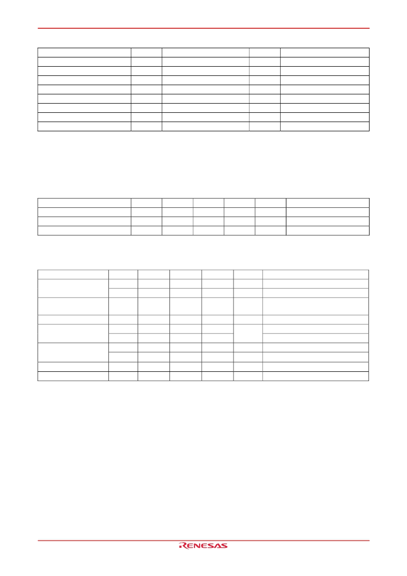
Absolute Maximum Ratings
Item
Symbol
V
DD
V
I
V
O
I
IK
I
OK
I
O
P
W
T
stg
Ratings
–0.5 to 4.6
–0.5 to 4.6
–0.5 to V
DD
+0.5
–50
–50
±
50
0.2
–65 to +150
Unit
V
V
V
mA
mA
mA
W
°
C
Conditions
Supply voltage
Input voltage
Output voltage
Input clamp current *
1
Output clamp current *
1
Continuous output current
Maximum power dissipation
Storage temperature
Notes: Stresses beyond those listed under "absolute maximum ratings" may cause permanent damage to the device.
These are stress ratings only, and functional operation of the device at these or any other conditions beyond
those indicated under “recommended operating conditions” is not implied.
1. The input and output negative voltage ratings may be exceeded if the input and output clamp current ratings
are observed.
Recommended Operating Conditions
V
I
< 0
V
O
< 0
V
O
= 0 to V
DD
T
a
= 25°C (in still air)
Item
Symbol
V
DD
T
a
Min
2.7
–0.3
–10
Typ
3.3
—
—
Max
3.6
V
DD
+0.3
75
Unit
V
V
°
C
Conditions
Supply voltage
DC input signal voltage
Operating temperature
DC Electrical Characteristics
T
a
=
–10 to 75
°
C, V
DD
=
2.7 to 3.6 V
Test Conditions
IN,
PDWN
, SEL, DIV2 pins
IN,
PDWN
, SEL, DIV2 pins
V
I
= 0 V or 3.6 V,
IN,
PDWN
, SEL, DIV2 pins
IN,
PDWN
, SEL, DIV2 pins
V
OL
= 1 mA, V
DD
= 3.3 V, OUT pin
V
OH
= –1 mA, V
DD
= 3.3 V, OUT pin
V
OL
= 1.65 V, V
DD
= 3.3 V, OUT pin
V
OH
= 1.65 V, V
DD
= 3.3 V, OUT pin
OUT pin
Item
Symbol
V
IL
V
IH
Min
—
2.0
Typ
—
—
Max
0.8
—
Unit
V
V
Input voltage
Input current
I
I
—
—
±
100
μ
A
Input capacitance
C
I
V
OL
V
OH
I
OL
I
OH
R
pd
—
—
3
—
—
15
–15
30
100 k
—
0.5
V
DD
—
—
—
120 k
pF
Output voltage
V
DD
–0.2
—
—
—
80 k
V
mA
mA
Output current
Output impedance
Pull-down resister
Note: The condition of the minimum and maximum value must use the value specified under “Recommended
Operating Conditions”.
Parameters are target of design. Not 100% tested in production.
相关PDF资料 |
PDF描述 |
|---|---|
| RD151TS501USE | PLL clock generator series |
| RD151TS502US | PLL clock generator series |
| RD151TS502USE | PLL clock generator series |
| RD74HV1G00 | High-Voltage 2-input NAND gate |
| RD74HV1G00VSE | High-Voltage 2-input NAND gate |
相关代理商/技术参数 |
参数描述 |
|---|---|
| RD151TS501USE | 制造商:RENESAS 制造商全称:Renesas Technology Corp 功能描述:PLL clock generator series |
| RD151TS502US | 制造商:RENESAS 制造商全称:Renesas Technology Corp 功能描述:PLL clock generator series |
| RD151TS502USE | 制造商:RENESAS 制造商全称:Renesas Technology Corp 功能描述:PLL clock generator series |
| RD-1524D | 制造商:RECOM 制造商全称:Recom International Power 功能描述:2 Watt SIP7 & DIP14 Dual Output |
| RD-1524DHP | 制造商:RECOM 制造商全称:Recom International Power 功能描述:2 Watt SIP7 & DIP14 Dual Output |
发布紧急采购,3分钟左右您将得到回复。