- 您现在的位置:买卖IC网 > PDF目录378128 > RDA012M4-DI (Electronic Theatre Controls, Inc.) 12 Bit 1.3 GS/s 4:1 MUXDAC PDF资料下载
参数资料
| 型号: | RDA012M4-DI |
| 厂商: | Electronic Theatre Controls, Inc. |
| 英文描述: | 12 Bit 1.3 GS/s 4:1 MUXDAC |
| 中文描述: | 12位1.3 GS / s的4:1 MUXDAC |
| 文件页数: | 7/12页 |
| 文件大小: | 392K |
| 代理商: | RDA012M4-DI |
RDA012M4 DATASHEET
DS_0012PB1-2805
Rockwell Scientific reserves the right to make changes to its product specifications at any time without notice.
The information furnished herein is believed to be accurate; however, no responsibility is assumed for its use.
Page 7 of 12
Theory of Operation
For best dynamic and static performance, the
DAC employs 6-bit segmentation. The 3.3V
NMOS compatible 12-bit digital data inputs are
latched by a master-slave flip-flop immediately
after the input buffer to reduce the data skew.
The four-channel data are combined together by
the 48:12 MUX and latched again. The 6 MSB
data bits are decoded into thermometer code by
a two-stage decoding block, and the 6 LSB data
bits are transported through the delay equalizer
block. The digital data are synchronized again
by a second master slave flip-flop to reduce the
switching glitch. The decoded 6 MSB data drive
63 identical current switches, and the 6 LSB
data drive 6 current switches. The output nodes
from the LSB current switches are connected to
the analog output through an R-2R ladder to
generate the binary output.
The DAC output full-scale voltage follows the
relationship V
FS
= 0.3xV
REF.
An internal
reference circuit with approximately -10dB
supply rejection is integrated on chip for
application convenience. The reference pin is
provided
for
monitoring
purposes. To band-limit the noise on the
reference voltage, the reference pin should be
bypassed to the GNDA node with capacitance >
100pF. The VREF pin can also be used to
override the internal reference with an accurate,
temperature-compensated
reference.
and
for
bypass
external
voltage
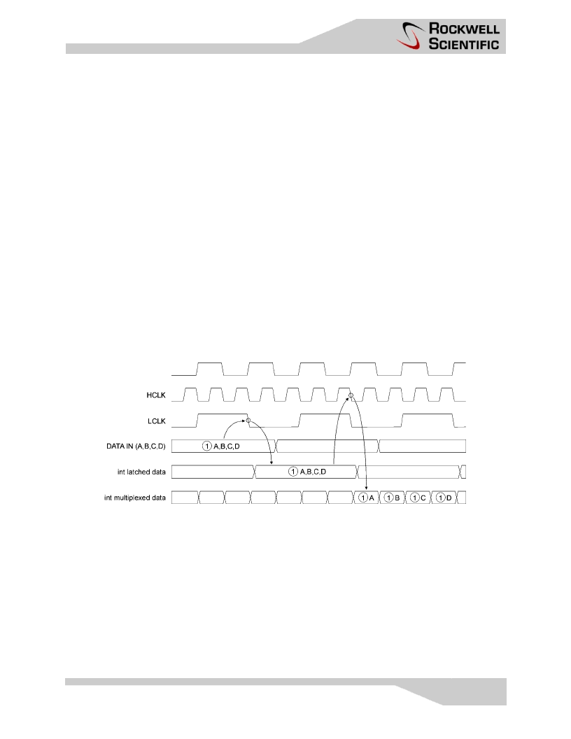
The timing diagram is shown in figure 3. The
1.3GHz external clock (HCLKI) is divided by 2
and 4 resulting in the MUX internal selection
signals S0 and S1. A low-speed clock (LCLKO)
is provided to drive the external digital. The
four-channel data input are latched with an
internal clock that is synchronized with the
LCLKO. Controlled by S0 and S1, input data are
fed to the 1.3GS/s DAC in the order shown.
Figure 4 - Input Timing Diagram.
相关PDF资料 |
PDF描述 |
|---|---|
| RDA012M4-HD | 12 Bit 1.3 GS/s 4:1 MUXDAC |
| RDL60V | RESETABLE FUSES |
| RDL60V010 | RESETABLE FUSES |
| RDL60V017 | RESETABLE FUSES |
| RDL60V185 | RESETABLE FUSES |
相关代理商/技术参数 |
参数描述 |
|---|---|
| RDA012M4-HD | 制造商:未知厂家 制造商全称:未知厂家 功能描述:12 Bit 1.3 GS/s 4:1 MUXDAC |
| RDA012M4MS | 制造商:未知厂家 制造商全称:未知厂家 功能描述:12 Bit 1.3 GS/s Master-Slave 4:1 MUXDAC |
| RDA012M4MS-DI | 制造商:未知厂家 制造商全称:未知厂家 功能描述:12 Bit 1.3 GS/s Master-Slave 4:1 MUXDAC |
| RDA012M4MS-HD | 制造商:未知厂家 制造商全称:未知厂家 功能描述:12 Bit 1.3 GS/s Master-Slave 4:1 MUXDAC |
| RDA1005LTR7 | 制造商:RF Micro Devices Inc 功能描述:IC AMP DVGA 32-MCM 5.2X5.2 |
发布紧急采购,3分钟左右您将得到回复。