参数资料
| 型号: | RDK-160 |
| 厂商: | Power Integrations |
| 文件页数: | 1/18页 |
| 文件大小: | 0K |
| 描述: | KIT REF DESIGN LINKSWITCH 2 |
| 应用说明: | LinkSwitch-II Family, Appl Note AN-44 |
| 设计资源: | RDR-157, 2.78W USB Charger Using LNK613DG RDR-158, 5W Charger Using LNK616PG RDR-159, 2.4W Charger Using LNK603DG |
| 标准包装: | 1 |
| 系列: | LinkSwitch-II |
| 主要目的: | AC/DC,主面 |
| 输出及类型: | 1,隔离 |
| 输入电压: | 85 ~ 265VAC |
| 稳压器拓扑结构: | 回扫 |
| 板类型: | 裸(未填充)和完全填充 |
| 已供物品: | 3 块装有元件的板,3 裸板,文档,样品 IC,软件 |
| 已用 IC / 零件: | LNK603,LNK604,LNK605,LNK606,LNK613,LNK614,LNK615,LNK616 |
| 相关产品: | 732-2247-ND - TRANS OFF LINE POWER PI LNK616 732-2246-ND - TRANS OFF LINE POWER PI LNK613 732-2245-ND - TRANS OFF LINE POWER PI LNK603 732-2244-ND - TRANS OFF LINE POWER PI LNK605 LNK616GG-TL-ND - IC OFFLINE SWIT CV/CC HV 8SMD LNK606GG-TL-ND - IC OFFLINE SWIT CV/CC HV 8SOIC LNK615DG-TL-ND - IC OFFLINE SWIT CV/CC HV 8SOIC LNK605DG-TL-ND - IC OFFLINE SWIT CV/CC HV 8SOIC LNK614DG-TL-ND - IC OFFLINE SWIT CV/CC HV 8SOIC LNK604DG-TL-ND - IC OFFLINE SWIT CV/CC HV 8SOIC 更多... |
| 其它名称: | 596-1235 |
�� �
�
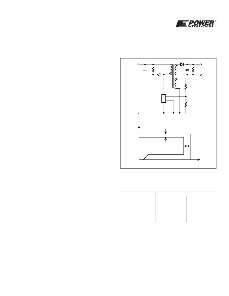
�LinkSwitch-II� Family�
�LNK603-606/613-616�
�?�
�Energy-Efficient,� Accurate� CV/CC� Switcher�
�for� Adapters� and� Chargers�
�Product� Highlights�
�Dramatically� Simplifies� CV/CC� Converters�
�?� Eliminates� optocoupler� and� all� secondary� CV/CC� control� circuitry�
�?� Eliminates� all� control� loop� compensation� circuitry�
�Advanced� Performance� Features�
�?� Compensates� for� transformer� inductance� tolerances�
�?� Compensates� for� input� line� voltage� variations�
�?� Compensates� for� cable� voltage� drop� (LNK61X� series)�
�?� Compensates� for� external� component� temperature� variations�
�?� Very� tight� IC� parameter� tolerances� using� proprietary� trimming�
�technology�
�Wide� Range�
�High� Voltage�
�DC� Input�
�LinkSwitch-II�
�D�
�S�
�FB�
�BP/M�
�?� Frequency� jittering� greatly� reduces� EMI� filter� cost�
�?� Even� tighter� output� tolerances� achievable� with� external� resistor�
�selection/trimming�
�?� Programmable� switching� frequency� up� to� 85� kHz� to� reduce�
�(a)� Typical� Application� Schematic�
�PI-4960-011510�
�transformer� size�
�Advanced� Protection/Safety� Features�
�?� Auto-restart� protection� reduces� power� delivered� by� >95%� for�
�output� short� circuit� and� control� loop� faults� (open� and� shorted�
�components)�
�?� Hysteretic� thermal� shutdown� –� automatic� recovery� reduces�
�power� supply� returns� from� the� field�
�?� Meets� high� voltage� creepage� requirements� between� DRAIN� and�
�V� O�
�±5%�
�±10%�
�all� other� pins� both� on� the� PCB� and� at� the� package�
�EcoSmart� ?� –� Energy� Efficient�
�PI-4906-041008�
�(b)� Output� Characteristic�
�I� O�
�?� Easily� meets� all� global� energy� efficiency� regulations�
�?� No-load� consumption� below� 30� mW� at� 230� VAC� with� optional�
�external� bias� winding�
�Figure� 1.�
�Typical� Application/Performance� –� Not� a� Simplified� Circuit� (a)� and�
�Output� Characteristic� Envelope� (b).� (see� Application� Section� for�
�more� information).�
�?� ON/OFF� control� provides� constant� efficiency� down� to� very� light�
�loads� –� ideal� for� CEC� and� ENERGY� STAR� 2.0� regulations�
�Output� Power� Table�
�Adapter�
�?� No� current� sense� resistors� –� maximizes� efficiency�
�Green� Package�
�?� Halogen� free� and� RoHS� compliant� package�
�Applications�
�?� Chargers� for� cell/cordless� phones,� PDAs,� MP3/portable� audio�
�devices,� adapters,� LED� drivers,� etc.�
�Product� 3�
�LNK603/613PG/DG�
�LNK604/614PG/DG�
�LNK605/615PG/DG�
�LNK606/616PG/GG/DG�
�2.5� W�
�3.5� W�
�4.5� W�
�5.5� W�
�1�
�85-265� VAC�
�Open� Frame� 2�
�3.3� W�
�4.1� W�
�5.1� W�
�6.1� W�
�Description�
�The� LinkSwitch-II� dramatically� simplifies� low� power� CV/CC�
�charger� designs� by� eliminating� an� optocoupler� and� secondary�
�control� circuitry.� The� device� introduces� a� revolutionary� control�
�technique� to� provide� very� tight� output� voltage� and� current�
�regulation,� compensating� for� transformer� and� internal� parameter�
�tolerances� along� with� input� voltage� variations.�
�The� device� incorporates� a� 700� V� power� MOSFET,� a� novel� ON/OFF�
�control� state� machine,� a� high� voltage� switched� current� source� for�
�self� biasing,� frequency� jittering,� cycle-by-cycle� current� limit� and�
�hysteretic� thermal� shutdown� circuitry� onto� a� monolithic� IC.�
�www.powerint.com�
�Table� 1.� Output� Power� Table.�
�Notes:�
�1.� Minimum� continuous� power� in� a� typical� non-ventilated� enclosed� adapter�
�measured� at� +50� °C� ambient,� device,� T� J� <100� °C.�
�2.� Maximum� practical� continuous� power� in� an� open� frame� design� with� adequate�
�heatsinking,� measured� at� 50� °C� ambient� (see� Key� Applications� Considerations�
�section� for� more� information).�
�3.� Packages:� P:� DIP-8C,� G:� SMD-8C,� D:� SO-8C.�
�January� 2010�
�相关PDF资料 |
PDF描述 |
|---|---|
| RDK-236 | KIT REF DESIGN PFS714EG |
| RECE-20279-001E-01 | RCPT IPEX MHF |
| RF2594-000 | BD540-30 |
| RF2873-000 | POLYSWITCH 1.25A RESET FUSE RAD |
| RGEF1000-1 | POLYSWITCH PTC RESET 10A HOLD |
相关代理商/技术参数 |
参数描述 |
|---|---|
| RDK-189 | 功能描述:KIT REF DESIGN FOR PLC810 RoHS:是 类别:编程器,开发系统 >> 评估板 - DC/DC 与 AC/DC(离线)SMPS 系列:HiperPLC™ 产品培训模块:Obsolescence Mitigation Program 标准包装:1 系列:True Shutdown™ 主要目的:DC/DC,步升 输出及类型:1,非隔离 功率 - 输出:- 输出电压:- 电流 - 输出:1A 输入电压:2.5 V ~ 5.5 V 稳压器拓扑结构:升压 频率 - 开关:3MHz 板类型:完全填充 已供物品:板 已用 IC / 零件:MAX8969 |
| RDK-193 | 功能描述:LED 照明开发工具 LED Drvr Ref Des LinkSwitch-PH RoHS:否 制造商:Fairchild Semiconductor 产品:Evaluation Kits 用于:FL7732 核心: 电源电压:120V 系列: 封装: |
| RDK-194 | 功能描述:电源管理IC开发工具 LED Drvr Ref Des LinkSwitch-PH RoHS:否 制造商:Maxim Integrated 产品:Evaluation Kits 类型:Battery Management 工具用于评估:MAX17710GB 输入电压: 输出电压:1.8 V |
| RDK-195 | 功能描述:LED 照明开发工具 RefDesign 90-265V.5A OutputLinkSwitch-PH RoHS:否 制造商:Fairchild Semiconductor 产品:Evaluation Kits 用于:FL7732 核心: 电源电压:120V 系列: 封装: |
| RDK-201 | 功能描述:电源管理IC开发工具 LinkSwitch CV Reference Design Kit RoHS:否 制造商:Maxim Integrated 产品:Evaluation Kits 类型:Battery Management 工具用于评估:MAX17710GB 输入电压: 输出电压:1.8 V |
发布紧急采购,3分钟左右您将得到回复。