- 您现在的位置:买卖IC网 > PDF目录225034 > REF3333AIDCKT (TEXAS INSTRUMENTS INC) 1-OUTPUT THREE TERM VOLTAGE REFERENCE, 3.3 V, PDSO3 PDF资料下载
参数资料
| 型号: | REF3333AIDCKT |
| 厂商: | TEXAS INSTRUMENTS INC |
| 元件分类: | 基准电压源/电流源 |
| 英文描述: | 1-OUTPUT THREE TERM VOLTAGE REFERENCE, 3.3 V, PDSO3 |
| 封装: | GREEN, SC-70, 3 PIN |
| 文件页数: | 20/20页 |
| 文件大小: | 580K |
| 代理商: | REF3333AIDCKT |
www.ti.com
POWER DISSIPATION
APPLICATION CIRCUITS
T =T +P q
J
A
D
JA
(2)
NOISE PERFORMANCE
R
3
R
2
V
IN
+2.7V
Enable
(1)
OPA333,
OPA363,
OPA369
or
R
66.5
1
W
C
1.5nF
1
C
1 F
2
m
P1.2
VREF
A0+
REF3312
+2.7V
V
CC
V
SS
16-Bit
ADC
MSP430x20x3PW
SBOS392A – AUGUST 2007 – REVISED SEPTEMBER 2007
The REF33xx family is specified to deliver current
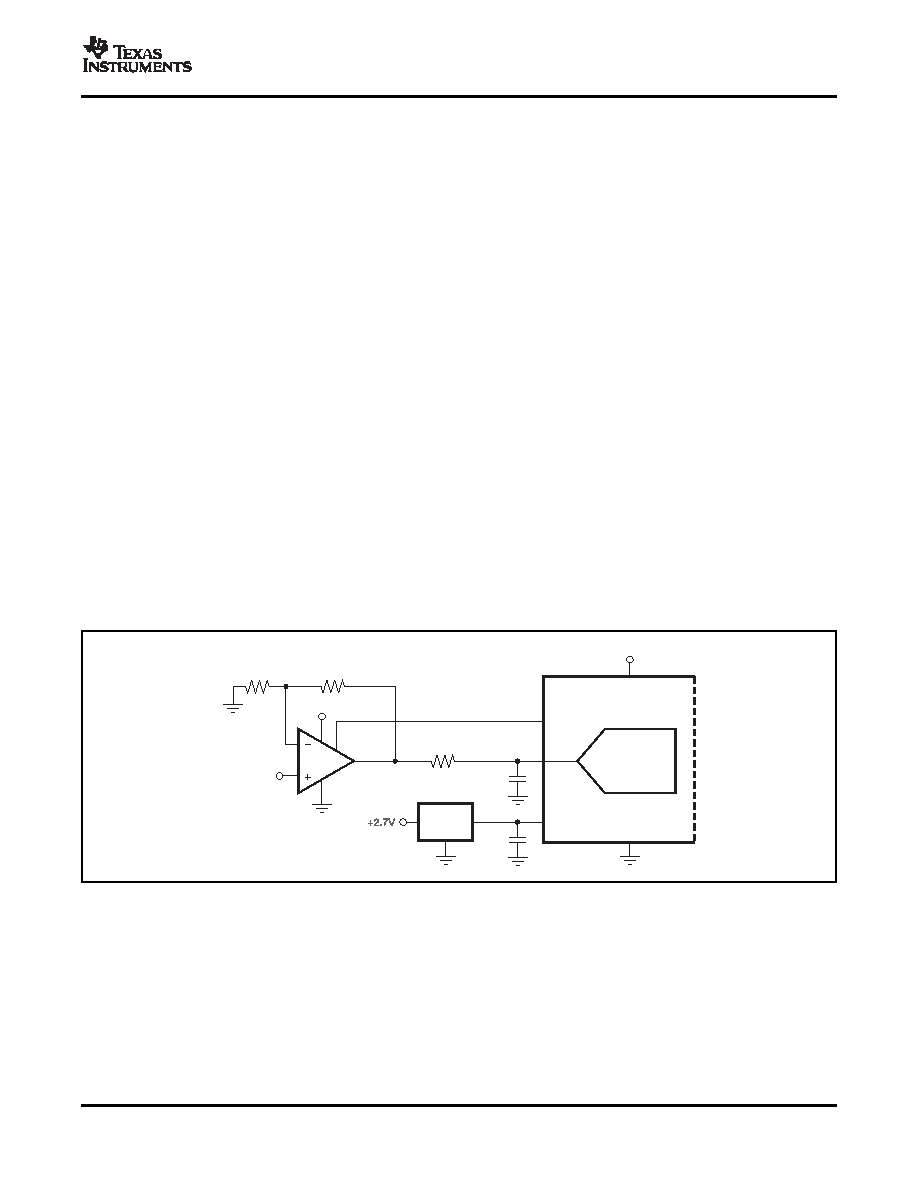
Figure 20 shows a simple application circuit where
loads of ±5mA over the specified input voltage range.
low-power components are used to create a signal
The temperature of the device increases according to
chain. The analog input signal is buffered with either
reference voltage created from REF3312 provides a
stable, high-accuracy, low-drift reference voltage to
the MSP430 using much less power than the
Where:
MSP430 internal reference. The reference voltage is
TJ = Junction temperature (°C)
used by the internal, 16-bit analog-to-digital converter
TA = Ambient temperature (°C)
(ADC) to accurately convert the analog input signal.
PD = Power dissipation (W)
The configuration in Figure 20 presents an example
Where PD = VIN × IQ + (VIN – VOUT) IOUT
of a unipolar signal chain.
θJA = Junction-to-ambient thermal resistance
An example of a bipolar configuration is illustrated in
(
°C/W)
Figure 21. The analog input signal (±2.5V) is offset
and attenuated so that it matches the analog input of
The REF33xx junction temperature must not exceed
the 16-bit ADC on the MSP430. The negative input of
the absolute maximum rating of +150
°C.
the ADC is offset by 0.62V, creating a digital code
that corresponds to the analog input voltage. In this
configuration, two reference voltages are used. The
Typical 0.1Hz to 10Hz voltage noise for each member
REF3312 creates a 1.25V reference input to the ADC
of the REF33xx family is specified in the Electrical
and is an offset point for the INA159. The same
Characteristics table. The noise voltage increases
voltage is used to create the offset voltage to the
with
output
voltage
and
operating
temperature.
negative input to the ADC. The REF3330 creates a
Additional filtering can be used to improve output
precise analog supply voltage of 3V. In this way, the
noise levels. Special attention should be taken to
high PSRR of the REF3330 helps to filter unwanted
ensure that the output impedance does not degrade
noise from the 3.3V digital supply.
output voltage accuracy.
(1)
Enable is a function of the OPA363 not available on the OPA333.
Figure 20. Unipolar Signal Chain Configuration
Copyright 2007, Texas Instruments Incorporated
9
相关PDF资料 |
PDF描述 |
|---|---|
| REF5045IDGKT | 1-OUTPUT THREE TERM VOLTAGE REFERENCE, 4.5 V, PDSO8 |
| REG101NA-2.5/250G4 | 2.5 V FIXED POSITIVE LDO REGULATOR, 0.13 V DROPOUT, PDSO5 |
| REG101NA-2.5/3KG4 | 2.5 V FIXED POSITIVE LDO REGULATOR, 0.13 V DROPOUT, PDSO5 |
| REG101NA-2.8/250G4 | 2.8 V FIXED POSITIVE LDO REGULATOR, 0.13 V DROPOUT, PDSO5 |
| REG101UA-2.5G4 | 2.5 V FIXED POSITIVE LDO REGULATOR, 0.13 V DROPOUT, PDSO8 |
相关代理商/技术参数 |
参数描述 |
|---|---|
| REF3333AIDCKTG4 | 功能描述:基准电压& 基准电流 30ppm/C Drift 3.9uA Vltg Ref RoHS:否 制造商:STMicroelectronics 产品:Voltage References 拓扑结构:Shunt References 参考类型:Programmable 输出电压:1.24 V to 18 V 初始准确度:0.25 % 平均温度系数(典型值):100 PPM / C 串联 VREF - 输入电压(最大值): 串联 VREF - 输入电压(最小值): 分流电流(最大值):60 mA 最大工作温度:+ 125 C 封装 / 箱体:SOT-23-3L 封装:Reel |
| REF3425IDBVR | 功能描述:REF3425 - 20 PPM/C IQ 85UA 制造商:texas instruments 系列:* 包装:剪切带(CT) 零件状态:在售 安装类型:表面贴装 封装/外壳:SOT-23-6 供应商器件封装:SOT-23-6 标准包装:1 |
| REF401 | 制造商:General Tools 功能描述:GLYCOL REFRACTOMETER TO MEASURE FREEZING POINT (-60 TO 32 F) |
| REF43 | 制造商:AD 制造商全称:Analog Devices 功能描述:+2.5V Low Power Precision Voltage Reference |
| REF-43 | 制造商:AD 制造商全称:Analog Devices 功能描述:+2.5V Low Power Precision Voltage Reference |
发布紧急采购,3分钟左右您将得到回复。