- 您现在的位置:买卖IC网 > PDF目录376305 > REG101 (Texas Instruments, Inc.) DMOS 100mA Low-Dropout Regulator PDF资料下载
参数资料
| 型号: | REG101 |
| 厂商: | Texas Instruments, Inc. |
| 英文描述: | DMOS 100mA Low-Dropout Regulator |
| 中文描述: | 的DMOS 100mA的低压差稳压器 |
| 文件页数: | 11/15页 |
| 文件大小: | 277K |
| 代理商: | REG101 |
REG101
SBVS026C
11
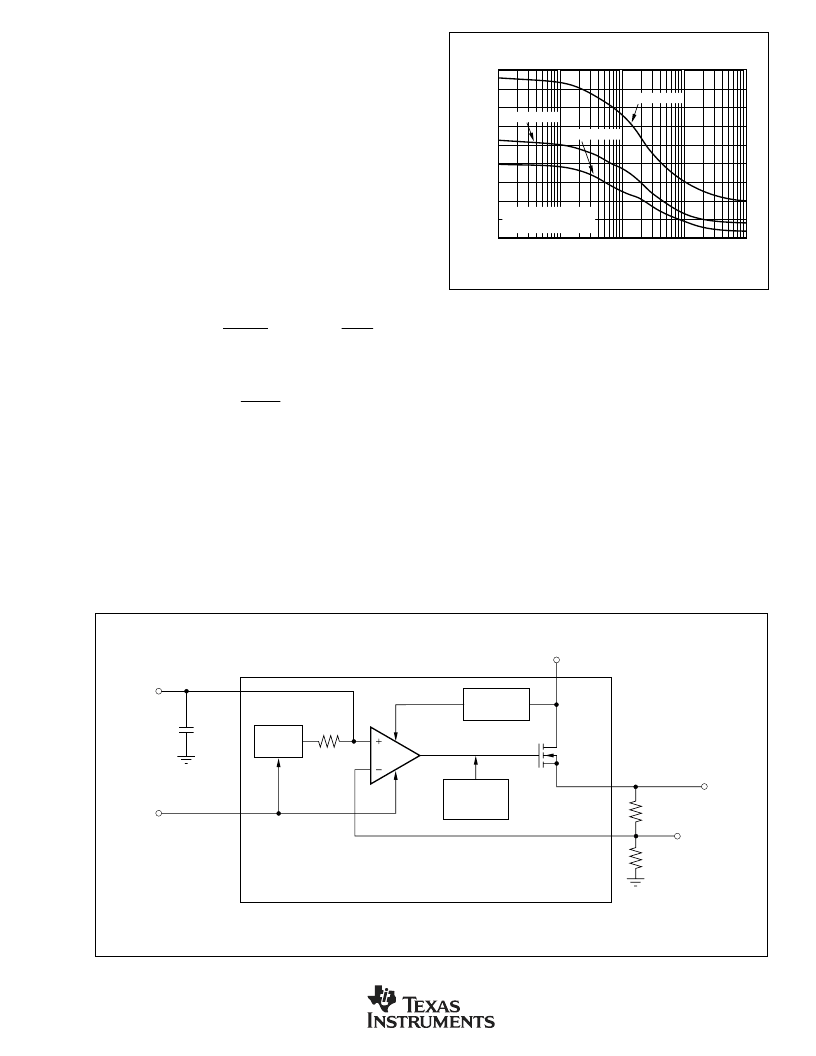
FIGURE 4. Block Diagram.
FIGURE 5. Output Noise versus Noise Reduction Capacitor.
ENABLE
The Enable pin is active HIGH and compatible with stan-
dard TTL-CMOS levels. Inputs below 0.5V (max) turn the
regulator off and all circuitry is disabled. Under this condi-
tion, ground pin current drops to approximately 10nA. When
a pull-up resistor is used, and operation down to V
IN
= 1.8V
is required, use values < 50k
.
OUTPUT NOISE
A precision band-gap reference is used for the internal
reference voltage, V
REF
. This reference is the dominant
noise source within the REG101 and it generates approxi-
mately 29
μ
Vrms in the 10Hz to 100kHz bandwidth at the
reference output. The regulator control loop gains up the
reference noise, so that the noise voltage of the regulator is
approximately given by:
V = 29 VrmsR +R
R2
VrmsV
μ
=
29
V
1
2
OUT
REF
Since the value of V
REF
is 1.267V, this relationship reduces to:
V = 23
Vrms
V
V
OUT
μ
Connecting a capacitor, C
NR
, from the Noise Reduction (NR)
pin to ground, as shown in Figure 4, forms a low-pass filter for
the voltage reference. For C
NR
= 10nF, the total noise in the
10Hz to 100kHz bandwidth is reduced by approximately a
factor of 2.8 for V
O
= 3.3V. This noise reduction effect is
shown in Figure 5 and as “RMS Noise Voltage vs CNR” in the
Typical Characteristics section.
Noise can be further reduced by carefully choosing an
output capacitor, C
OUT
. Best overall noise performance is
achieved with very low (< 0.22
μ
F) or very high (> 2.2
μ
F)
values of C
OUT
. See “RMS Noise Voltage vs C
OUT
” in the
Typical Characteristics section.
The REG101 utilizes an internal charge pump to develop an
internal supply voltage sufficient to drive the gate of the
DMOS pass element above V
IN
. The charge-pump switch-
ing noise (nominal switching frequency = 2MHz) is not
measurable at the output of the regulator over most values of
C
OUT
and I
OUT
.
The REG101 adjustable version does not have the noise-
reduction pin available, however, the adjust pin is the sum-
ming junction of the error amplifier. A capacitor, C
FB
,
connected from the output to the adjust pin will reduce both
the output noise and the peak error from a load transient. See
the typical characteristics for output noise performance.
Over Current
Over Temp
Protection
V
(1.26V)
Low Noise
Charge Pump
DMOS
Pass
Transistor
R
1
NOTE: R
and R
are internal
on fixed output versions.
V
OUT
Adj
(Adjustable
Versions)
R
2
NR
(fixed output
versions only)
Enable
REG101
V
IN
C
(optional)
1
10
1k
100
10k
110
100
90
80
70
60
50
40
30
20
N
μ
V
C
NR
(pF)
RMS NOISE VOLTAGE vs C
NR
C
= 0
μ
F
10Hz < BW < 100kHz
REG101-5.0
REG101-2.5
REG101-3.3
相关PDF资料 |
PDF描述 |
|---|---|
| REG102UA-2.8 | DMOS 250mA Low-Dropout Regulator |
| REG102UA-2.85 | DMOS 250mA Low-Dropout Regulator |
| REG102GA-2.8 | DMOS 250mA Low-Dropout Regulator |
| REG102 | DMOS 250mA Low-Dropout Regulator |
| REG113 | DMOS 400mA Low-Dropout Regulator(DMOS 400mA 低压差稳压器) |
相关代理商/技术参数 |
参数描述 |
|---|---|
| REG101_05 | 制造商:TI 制造商全称:Texas Instruments 功能描述:DMOS 100mA Low-Dropout Regulator |
| REG101-25 | 制造商:未知厂家 制造商全称:未知厂家 功能描述:DMOS 100mA Low Dropout (LDO) Regulator |
| REG101-28 | 制造商:未知厂家 制造商全称:未知厂家 功能描述:DMOS 100mA Low Dropout (LDO) Regulator |
| REG101-285 | 制造商:未知厂家 制造商全称:未知厂家 功能描述:DMOS 100mA Low Dropout (LDO) Regulator |
| REG101-3 | 制造商:未知厂家 制造商全称:未知厂家 功能描述:DMOS 100mA Low Dropout (LDO) Regulator |
发布紧急采购,3分钟左右您将得到回复。