- 您现在的位置:买卖IC网 > PDF目录225035 > REG103FA-2.7 (TEXAS INSTRUMENTS INC) 2.7 V FIXED POSITIVE LDO REGULATOR, 0.2 V DROPOUT, PSSO5 PDF资料下载
参数资料
| 型号: | REG103FA-2.7 |
| 厂商: | TEXAS INSTRUMENTS INC |
| 元件分类: | 固定正电压单路输出LDO稳压器 |
| 英文描述: | 2.7 V FIXED POSITIVE LDO REGULATOR, 0.2 V DROPOUT, PSSO5 |
| 封装: | PLASTIC, TO-263, D2PAK, 5 PIN |
| 文件页数: | 2/26页 |
| 文件大小: | 830K |
| 代理商: | REG103FA-2.7 |
REG103
10
SBVS010D
Since the value of VREF is 1.295V, this relationship reduces to:
V
Vrms
V
N
OUT
=
35
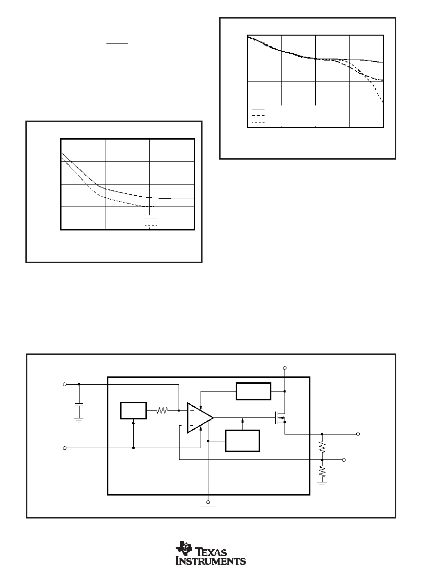
Connecting a capacitor, CNR, from the Noise-Reduction
(NR) pin to ground, can reduce the output noise voltage.
Adding CNR, as shown in Figure 7, forms a low-pass filter
for the voltage reference. For CNR = 10nF, the total noise in
the 10Hz to 100kHz bandwidth is reduced by approximately
a factor of 3.5, as shown in Figure 8.
FIGURE 7. Block Diagram.
Over Current
Over Temp
Protection
V
REF
(1.295V)
Low Noise
Charge Pump
DMOS
Output
R
1
NOTE: R
1 and R2 are internal
on fixed output versions.
V
OUT
Adj
(Adjustable
Versions)
R
2
NR
(fixed output
versions only)
ENABLE
REG103
V
IN
ERROR
C
NR
(optional)
FIGURE 8. Output Noise versus Noise-Reduction Capacitor.
0.001
0.01
0.1
1
45
35
25
Output
Noise
Voltage
(
V
RMS
10Hz
-
100kHz)
C
NR (F)
C
OUT = 0
C
OUT = 10F
FIGURE 9. Output Noise Density on Adjustable Versions.
100
10
1000
10000
100000
10.0
1.0
0.1
nV/
√Hz
Frequency
C
OUT = 0, CFB = 0
C
OUT = 0, CFB = 0.01F
C
OUT = 10F, CFB = 0.01F
The REG103 adjustable version does not have the noise-
reduction pin available, however, the adjust pin is the sum-
ming junction of the error amplifier. A capacitor, CFB,
connected from the output to the adjust pin will reduce both
the output noise and the peak error from a load transient.
Figure 9 shows improved output noise performance for two
capacitor combinations.
The REG103 utilizes an internal charge pump to develop an
internal supply voltage sufficient to drive the gate of the
DMOS pass element above VIN. The charge-pump switch-
ing noise (nominal switching frequency = 2MHz) is not
measurable at the output of the regulator.
DROP-OUT VOLTAGE
The REG103 uses an N-channel DMOS as the “pass”
element. When the input voltage is within a few hundred
millivolts of the output voltage, the DMOS device behaves
like a resistor. Therefore, for low values of VIN to VOUT, the
regulator’s input-to-output resistance is the RdsON of the
DMOS pass element (typically 230m
). For static (DC)
loads, the REG103 will typically maintain regulation down
to VIN to VOUT voltage drop of 115mV at full-rated output
current. In Figure 10, the bottom line (DC dropout) shows
the minimum VIN to VOUT voltage drop required to prevent
drop-out under DC load conditions.
相关PDF资料 |
PDF描述 |
|---|---|
| REG103FA-3.3/500 | 3.3 V FIXED POSITIVE LDO REGULATOR, 0.2 V DROPOUT, PSSO5 |
| REG103FA-3.3 | 3.3 V FIXED POSITIVE LDO REGULATOR, 0.2 V DROPOUT, PSSO5 |
| REG103GA-3.3 | 3.3 V FIXED POSITIVE LDO REGULATOR, 0.2 V DROPOUT, PDSO6 |
| REG103GA-5/2K5 | 5 V FIXED POSITIVE LDO REGULATOR, 0.25 V DROPOUT, PDSO6 |
| REG103GA-A/2K5 | 1.295 V-5.5 V ADJUSTABLE POSITIVE LDO REGULATOR, 0.2 V DROPOUT, PDSO6 |
相关代理商/技术参数 |
参数描述 |
|---|---|
| REG103FA-3 | 制造商:Rochester Electronics LLC 功能描述:- Bulk |
| REG103FA3.3 | 制造商: 功能描述: 制造商:undefined 功能描述: |
| REG103FA-3.3 | 制造商:BB 制造商全称:BB 功能描述:DMOS 500mA Low Dropout Regulator |
| REG103FA-3.3/500 | 功能描述:低压差稳压器 - LDO DMOS 500mA LDO Reg RoHS:否 制造商:Texas Instruments 最大输入电压:36 V 输出电压:1.4 V to 20.5 V 回动电压(最大值):307 mV 输出电流:1 A 负载调节:0.3 % 输出端数量: 输出类型:Fixed 最大工作温度:+ 125 C 安装风格:SMD/SMT 封装 / 箱体:VQFN-20 |
| REG103FA-3.3/500G3 | 功能描述:低压差稳压器 - LDO DMOS 500mA LDO Reg RoHS:否 制造商:Texas Instruments 最大输入电压:36 V 输出电压:1.4 V to 20.5 V 回动电压(最大值):307 mV 输出电流:1 A 负载调节:0.3 % 输出端数量: 输出类型:Fixed 最大工作温度:+ 125 C 安装风格:SMD/SMT 封装 / 箱体:VQFN-20 |
发布紧急采购,3分钟左右您将得到回复。