- 您现在的位置:买卖IC网 > PDF目录225035 > REG103FA-2.7 (TEXAS INSTRUMENTS INC) 2.7 V FIXED POSITIVE LDO REGULATOR, 0.2 V DROPOUT, PSSO5 PDF资料下载
参数资料
| 型号: | REG103FA-2.7 |
| 厂商: | TEXAS INSTRUMENTS INC |
| 元件分类: | 固定正电压单路输出LDO稳压器 |
| 英文描述: | 2.7 V FIXED POSITIVE LDO REGULATOR, 0.2 V DROPOUT, PSSO5 |
| 封装: | PLASTIC, TO-263, D2PAK, 5 PIN |
| 文件页数: | 3/26页 |
| 文件大小: | 830K |
| 代理商: | REG103FA-2.7 |
REG103
11
SBVS010D
FIGURE 11. Maximum Power Dissipation versus Ambient
Temperature for the Various Packages and
PCB Heat Sink Configurations.
6
5
4
3
2
1
0
Power
Dissipation
(W)
0
25
50
75
100
150
125
Ambient Temperature (
°C)
CONDITIONS
#1
#2
#3
#4
#5
CONDITION
PACKAGE
PCB AREA
JA
θ
1
DDPAK
4in2 Top Side Only
27
°C/W
2
SOT-223
4in2 Top Side Only
53
°C/W
3
DDPAK
None
65
°C/W
4
SOT-223
0.5in2 Top Side Only
110
°C/W
5
SO-8
None
150
°C/W
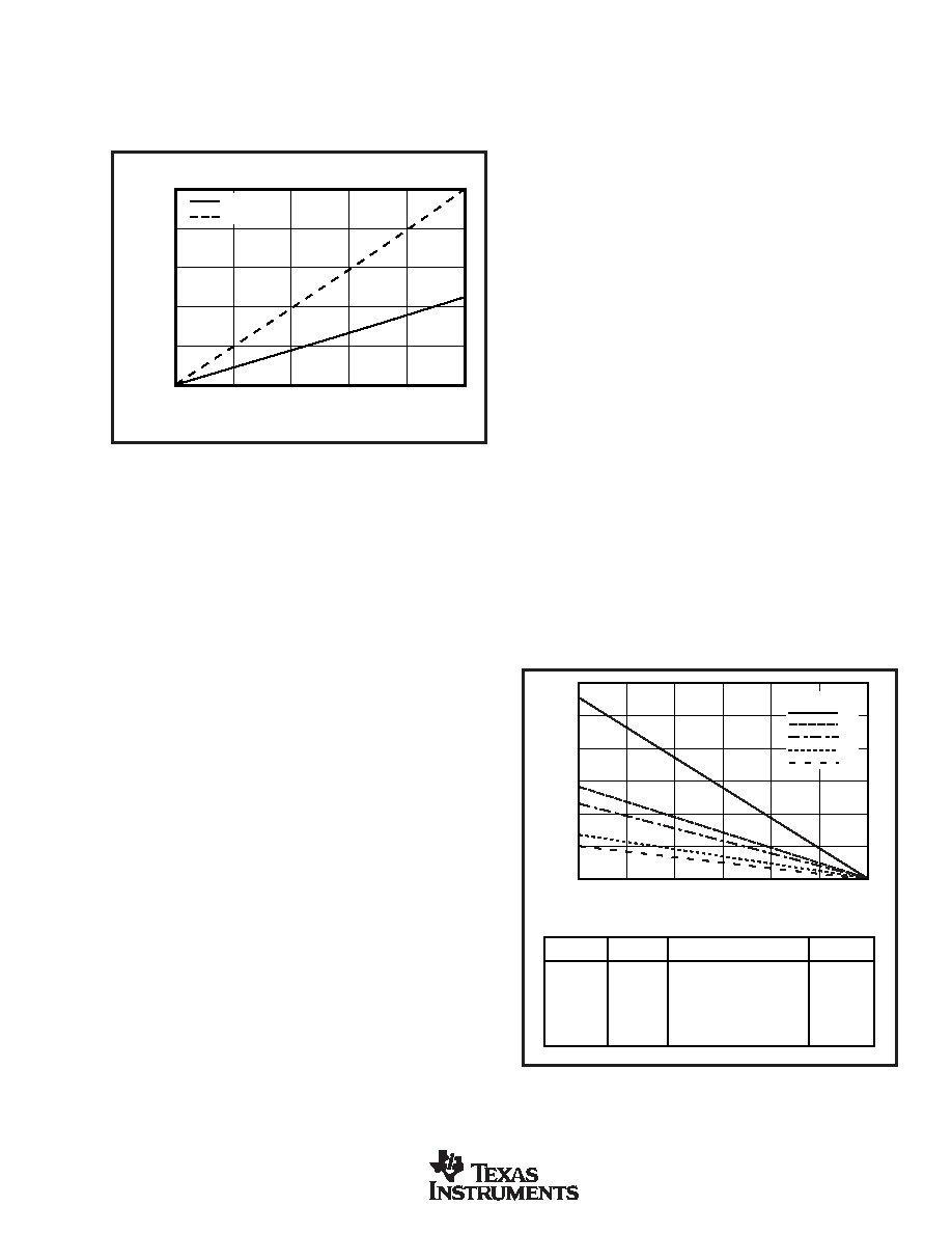
For large step changes in load current, the REG103 requires
a larger voltage drop across it to avoid degraded transient
response. The boundary of this “transient drop-out” region is
shown as the top line in Figure 10. Values of VIN to VOUT
voltage drop above this line insure normal transient response.
250
200
150
100
50
0
Drop-Out
Voltage
(mV)
0
100
200
300
400
500
I
OUT (mA)
REG103–3.3 at 25
°C
DC
Transient
FIGURE 10. Transient and DC Dropout.
In the transient dropout region between “DC” and “Tran-
sient”, transient response recovery time increases. The time
required to recover from a load transient is a function of both
the magnitude and rate of the step change in load current and
the available “headroom” VIN to VOUT voltage drop. Under
worst-case conditions (full-scale load change with VIN to
VOUT voltage drop close to DC dropout levels), the REG103
can take several hundred microseconds to re-enter the speci-
fied window of regulation.
TRANSIENT RESPONSE
The REG103 response to transient line and load conditions
improves at lower output voltages. The addition of a capaci-
tor (nominal value 10nF) from the output pin to ground may
improve the transient response. In the adjustable version, the
addition of a capacitor, CFB (nominal value 10nF), from the
output to the adjust pin will also improve the transient
response.
THERMAL PROTECTION
Power dissipated within the REG103 will cause the junction
temperature to rise. The REG103 has thermal shutdown
circuitry that protects the regulator from damage. The ther-
mal protection circuitry disables the output when the junc-
tion temperature reaches approximately 150
°C, allowing the
device to cool. When the junction temperature cools to
approximately 130
°C, the output circuitry is again enabled.
Depending on various conditions, the thermal protection
circuit may cycle on and off. This limits the dissipation of
the regulator, but may have an undesirable effect on the load.
Any tendency to activate the thermal protection circuit
indicates excessive power dissipation or an inadequate heat
sink. For reliable operation, junction temperature should be
limited to 125
°C, maximum. To estimate the margin of
safety in a complete design (including heat sink), increase
the ambient temperature until the thermal protection is
triggered. Use worst-case loads and signal conditions. For
good reliability, thermal protection should trigger more than
35
°C above the maximum expected ambient condition of
your application. This produces a worst-case junction tem-
perature of 125
°C at the highest expected ambient tempera-
ture and worst-case load.
The internal protection circuitry of the REG103 has been
designed to protect against overload conditions. It was not
intended to replace proper heat sinking. Continuously run-
ning the REG103 into thermal shutdown will degrade reli-
ability.
POWER DISSIPATION
The REG103 is available in three different package configu-
rations. The ability to remove heat from the die is different
for each package type and, therefore, presents different
considerations in the printed circuit board (PCB) layout. The
PCB area around the device that is free of other components
moves the heat from the device to the ambient air. While it
is difficult to impossible to quantify all of the variables in a
thermal design of this type, performance data for several
configurations are shown in Figure 11. In all cases, the PCB
copper area is bare copper, free of solder-resist mask, and
not solder plated. All examples are for 1-ounce copper.
Using heavier copper will increase the effectiveness in
moving the heat from the device. In those examples where
there is copper on both sides of the PCB, no connection has
been provided between the two sides. The addition of plated
through holes will improve the heat sink effectiveness.
相关PDF资料 |
PDF描述 |
|---|---|
| REG103FA-3.3/500 | 3.3 V FIXED POSITIVE LDO REGULATOR, 0.2 V DROPOUT, PSSO5 |
| REG103FA-3.3 | 3.3 V FIXED POSITIVE LDO REGULATOR, 0.2 V DROPOUT, PSSO5 |
| REG103GA-3.3 | 3.3 V FIXED POSITIVE LDO REGULATOR, 0.2 V DROPOUT, PDSO6 |
| REG103GA-5/2K5 | 5 V FIXED POSITIVE LDO REGULATOR, 0.25 V DROPOUT, PDSO6 |
| REG103GA-A/2K5 | 1.295 V-5.5 V ADJUSTABLE POSITIVE LDO REGULATOR, 0.2 V DROPOUT, PDSO6 |
相关代理商/技术参数 |
参数描述 |
|---|---|
| REG103FA-3 | 制造商:Rochester Electronics LLC 功能描述:- Bulk |
| REG103FA3.3 | 制造商: 功能描述: 制造商:undefined 功能描述: |
| REG103FA-3.3 | 制造商:BB 制造商全称:BB 功能描述:DMOS 500mA Low Dropout Regulator |
| REG103FA-3.3/500 | 功能描述:低压差稳压器 - LDO DMOS 500mA LDO Reg RoHS:否 制造商:Texas Instruments 最大输入电压:36 V 输出电压:1.4 V to 20.5 V 回动电压(最大值):307 mV 输出电流:1 A 负载调节:0.3 % 输出端数量: 输出类型:Fixed 最大工作温度:+ 125 C 安装风格:SMD/SMT 封装 / 箱体:VQFN-20 |
| REG103FA-3.3/500G3 | 功能描述:低压差稳压器 - LDO DMOS 500mA LDO Reg RoHS:否 制造商:Texas Instruments 最大输入电压:36 V 输出电压:1.4 V to 20.5 V 回动电压(最大值):307 mV 输出电流:1 A 负载调节:0.3 % 输出端数量: 输出类型:Fixed 最大工作温度:+ 125 C 安装风格:SMD/SMT 封装 / 箱体:VQFN-20 |
发布紧急采购,3分钟左右您将得到回复。