- 您现在的位置:买卖IC网 > PDF目录69322 > RH80536GE0362M (INTEL CORP) 1860 MHz, MICROPROCESSOR, CPGA478 PDF资料下载
参数资料
| 型号: | RH80536GE0362M |
| 厂商: | INTEL CORP |
| 元件分类: | 微控制器/微处理器 |
| 英文描述: | 1860 MHz, MICROPROCESSOR, CPGA478 |
| 封装: | FLIP CHIP, MICRO PGA-478 |
| 文件页数: | 11/30页 |
| 文件大小: | 887K |
| 代理商: | RH80536GE0362M |
第1页第2页第3页第4页第5页第6页第7页第8页第9页第10页当前第11页第12页第13页第14页第15页第16页第17页第18页第19页第20页第21页第22页第23页第24页第25页第26页第27页第28页第29页第30页
Datasheet
19
Electrical Specifications
3.5
Signal Terminations and Unused Pins
All RSVD (RESERVED) pins must remain unconnected. Connection of these pins to VCC, VSS, or
to any other signal (including each other) can result in component malfunction or incompatibility
with future Pentium M Processors. See Section 4.1 for a pin listing of the processor and the
location of all RSVD pins.
For reliable operation, always connect unused inputs or bidirectional signals to an appropriate
signal level. Unused active low AGTL+ inputs may be left as no connects if AGTL+ termination is
provided on the processor silicon. Unused active high inputs should be connected through a resistor
to ground (VSS). Unused outputs can be left unconnected.
The TEST1 and TEST2 pins must have a stuffing option connection to VSS separately via 1 k,
pull-down resistors.
3.6
FSB Frequency Select Signals (BSEL[1:0])
The BSEL[1:0] signals are used to select the frequency of the processor input clock (BCLK[1:0]).
These signals should be connected to the clock chip and Intel 915PM/GM and Intel 915GMS
Express chipset on the platform. The BSEL encoding for BCLK[1:0] is shown in Table 3-2.
3.7
FSB Signal Groups
In order to simplify the following discussion, the FSB signals have been combined into groups by
buffer type. AGTL+ input signals have differential input buffers, which use GTLREF as a reference
level. In this document, the term “AGTL+ Input” refers to the AGTL+ input group as well as the
AGTL+ I/O group when receiving. Similarly, “AGTL+ Output” refers to the AGTL+ output group
as well as the AGTL+ I/O group when driving.
With the implementation of a source synchronous data bus comes the need to specify two sets of
timing parameters. One set is for common clock signals which are dependant upon the rising edge
of BCLK0 (ADS#, HIT#, HITM#, etc.) and the second set is for the source synchronous signals
which are relative to their respective strobe lines (data and address) as well as the rising edge of
BCLK0. Asychronous signals are still present (A20M#, IGNNE#, etc.) and can become active at
any time during the clock cycle. Table 3-3 identifies which signals are common clock, source
synchronous, and asynchronous.
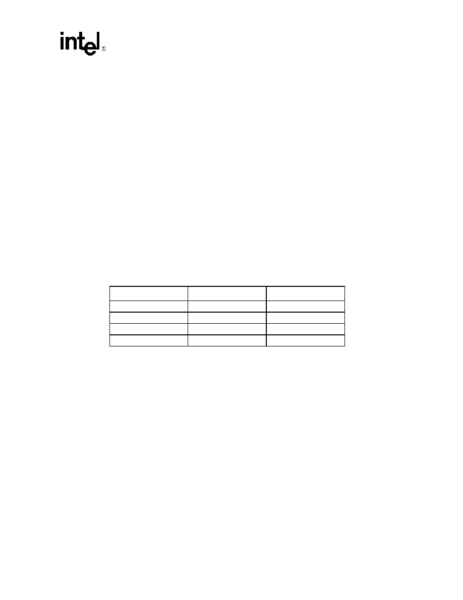
Table 3-2. BSEL[1:0] Encoding for BCLK Frequency
BSEL[1]
BSEL[0]
BCLK Frequency
L
H
100 MHz
L
133 MHz
H
L
RESERVED
H
RESERVED
相关PDF资料 |
PDF描述 |
|---|---|
| BX80536GE1733FJ | 1730 MHz, MICROPROCESSOR, CPGA478 |
| RJ80536GE0362M | 1860 MHz, MICROPROCESSOR, PBGA479 |
| RHFXH162373K-01Q | ALVC/VCX/A SERIES, DUAL 8-BIT DRIVER, TRUE OUTPUT, CDFP48 |
| RHRXH162373K-01Q | ALVC/VCX/A SERIES, DUAL 8-BIT DRIVER, TRUE OUTPUT, CDFP48 |
| RHRXH162373K01V | ALVC/VCX/A SERIES, DUAL 8-BIT DRIVER, TRUE OUTPUT, CDFP48 |
相关代理商/技术参数 |
参数描述 |
|---|---|
| RH80536GE0362M S L7S9 | 制造商:Intel 功能描述:MPU Pentium |
| RH80536GE0412M | 制造商:Rochester Electronics LLC 功能描述:PENTIUM M 0.09 MICRON 533MHZ 1.102V 478FCBGA - Bulk |
| RH80536GE0412M S L7EJ | 制造商:Intel 功能描述:32-Bit Microprocessor |
| RH80536GE0412M S L7SM | 制造商:Intel 功能描述:MPU Pentium? M Processor 760 90nm 2GHz 1.05V 479-Pin uFCBGA |
| RH80536GE0412M S LJ8S | 制造商:Intel 功能描述:DOTHAN; MPU PENTIUM M 90NM 2GHZ 1.05V 479PIN UFCBGA - Trays |
发布紧急采购,3分钟左右您将得到回复。