- 您现在的位置:买卖IC网 > PDF目录297328 > RV5C348A (RICOH COMPANY LTD) 4-WIRE SERIAL INTERFACE PDF资料下载
参数资料
| 型号: | RV5C348A |
| 厂商: | RICOH COMPANY LTD |
| 元件分类: | XO, clock |
| 英文描述: | 4-WIRE SERIAL INTERFACE |
| 中文描述: | 0 TIMER(S), REAL TIME CLOCK, PDSO10 |
| 封装: | 4 X 2.90 MM, 1.20 MM HEIGHT, 0.50 MM PITCH, SSOP-10 |
| 文件页数: | 14/45页 |
| 文件大小: | 1276K |
| 代理商: | RV5C348A |
第1页第2页第3页第4页第5页第6页第7页第8页第9页第10页第11页第12页第13页当前第14页第15页第16页第17页第18页第19页第20页第21页第22页第23页第24页第25页第26页第27页第28页第29页第30页第31页第32页第33页第34页第35页第36页第37页第38页第39页第40页第41页第42页第43页第44页第45页
Rx5C348A/B
Interfacing with the CPU
DATA TRANSFER FORMATS
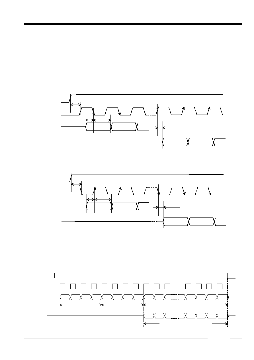
(1) Timing Between CE Pin Transition and Data Input / Output
The Rx5C348A/B adopts a 4-wire serial interface by which they use the CE (Chip Enable), SCLK (Serial Clock),
SI
(Serial Input), and SO (Serial Output) pins to receive and send data to and from the CPU.
The 4-wire serial
interface provides two types of input/output timings with which the SO pin output and the SI pin input are
synchronized with the rising or falling edges of the SCLK pin input, respectively, and vice versa.
The
Rx5C348A/B is configured to select either one of two different input/output timings depending on the level of the
SCLK pin in the low to high transition of the CE pin.
Namely, when the SCLK pin is held low in the low to high
transition of the CE pin, the models will select the timing with which the SO pin output is synchronized with the
rising edge of the SCLK pin input, and the SI pin input is synchronized with the falling edge of the SCLK pin input,
as illustrated in the timing chart below.
SCLK
SO
tDS
SI
CE
tCES
tDH
tRD
Conversely, when the SCLK pin is held high in the low to high transition of the CE pin, the models will select the
timing with which the SO pin output is synchronized with the falling edge of the SCLK pin input, and the SI pin
input is synchronized with the rising edge of the SCLK pin input, as illustrated in the timing chart below.
SCLK
SO
tDS
SI
CE
tCES
tDH
tRD
(2) Data Transfer Formats
Data transfer is commenced in the low to high transition of the CE pin input and completed in its high to low
transition.
Data transfer is conducted serially in multiple units of 1 byte (8 bits).
The former 4 bits are used to
specify in the Address Pointer a head address with which data transfer is to be commenced from the host.
The
latter 4 bits are used to select either reading data transfer or writing data transfer, and to set the Transfer Format
Register to specify an appropriate data transfer format.
All data transfer formats are designed to transfer the
most significant bit (MSB) first.
A2
CE
SCLK
SO
6
A1
A0
C3
C2
C1
C0
D7
D6
D3
D2
D1
D0
A3
7
58
2
3
1
23
1
4
D7
D6
D3
D2
D1
D0
Reading data transfer
Setting
the Address Pointer
Writing data transfer
Setting the Transfer
Format Register
SI
Two types of data transfer formats are available for reading data transfer and writing data transfer each.
12345
Rev.2.01
- 21 -
相关PDF资料 |
PDF描述 |
|---|---|
| RV5C348B | 4-WIRE SERIAL INTERFACE |
| RS9EM18M | RECTANGULAR ADAPTER |
| TDH25FJ1212 | RECTANGULAR ADAPTER |
| TDH25FJ4545K | RECTANGULAR ADAPTER |
| TDH25MJ12D | RECTANGULAR ADAPTER |
相关代理商/技术参数 |
参数描述 |
|---|---|
| RV5C348B | 制造商:RICOH 制造商全称:RICOH electronics devices division 功能描述:4-WIRE SERIAL INTERFACE REAL-TIME CLOCK ICs WITH VOLTAGE MONITORING FUNCTION |
| RV5C386A | 制造商:RICOH 制造商全称:RICOH electronics devices division 功能描述:I2C-bus Real-Time Clock ICs with Voltage Monitoring Function |
| RV5C386A_03 | 制造商:RICOH 制造商全称:RICOH electronics devices division 功能描述:I2C bus SERIAL INTERFACE REAL-TIME CLOCK IC WITH VOLTAGE MONITORING FUNCTION |
| RV5C386A-E2 | 制造商:RICOH 制造商全称:RICOH electronics devices division 功能描述:I2C-bus Real-Time Clock ICs with Voltage Monitoring Function |
| RV5C387A | 制造商:RICOH 制造商全称:RICOH electronics devices division 功能描述:I2C-bus Real-Time Clock ICs with Voltage Monitoring Function |
发布紧急采购,3分钟左右您将得到回复。