- 您现在的位置:买卖IC网 > PDF目录25640 > S-7750C71XX-HCT1 SPECIALTY MICROPROCESSOR CIRCUIT, PBGA16 PDF资料下载
参数资料
| 型号: | S-7750C71XX-HCT1 |
| 元件分类: | 微控制器/微处理器 |
| 英文描述: | SPECIALTY MICROPROCESSOR CIRCUIT, PBGA16 |
| 封装: | 1.93 X 2.07 MM, 0.6 MM HEIGHT, LEAD FREE, WLP-16 |
| 文件页数: | 18/44页 |
| 文件大小: | 563K |
| 代理商: | S-7750C71XX-HCT1 |
第1页第2页第3页第4页第5页第6页第7页第8页第9页第10页第11页第12页第13页第14页第15页第16页第17页当前第18页第19页第20页第21页第22页第23页第24页第25页第26页第27页第28页第29页第30页第31页第32页第33页第34页第35页第36页第37页第38页第39页第40页第41页第42页第43页第44页
PROGRAMMABLE PORT CONTROLLER (PORT EXPANDER WITH BUILT-IN E2PROM CIRCUIT)
Rev.2.0_00
S-7750C
Seiko Instruments Inc.
25
How to Use S-7750C
1. SDA I/O pin and SCL input pin
In consideration of I
2C-bus protocol function, the SDA I/O and SCL input pins*1 should be connected with a pull-up
resister of approx.1 to 5 k
Ω.
The S-7750C cannot transmit normally without using a pull-up resistor.
*1.
In the case that the SCL input pin of the S-7750C is connected to the tri-state output pin in the master device,
connect the SCL input pin with a pull-up resistor as well in order not to set the SCL input pin in high impedance.
This prevents the S-7750C from error caused by high impedance from the tri-state pin when resetting the master
device during the voltage drop.
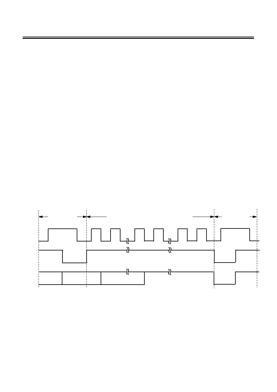
2. Reset after transmission interruption
The S-7750C does not have a pin to reset, but it generally resets the internal circuit by inputting a stop or start
condition. However, in case that transmission is interrupted, for example, only the master device is reset because the
power supply voltage drops during transmission; the internal circuit maintains the status before interruption. If the
status is that the SDA pin outputs “L” (outputs an acknowledge signal or in Read), the S-7750C does not perform the
next operation because it cannot receive a start or stop condition from the master device. Therefore it is necessary to
finish outputting an acknowledgment signal and the Read operation in SDA. Figure 31 shows how to reset.
First, input a start condition. (While the SDA pin is outputting “L”, the S-7750C does not go in the start condition but
this “L” output does not affect on the slave device.) Next, input clock (27 clocks) which is equivalent to 3-byte data
access from the SCL pin. During this procedure, pull up the SDA line which is connected closer to the master device.
Due to this, the SDA pin’s I/O prior to transmission interruption ends so that the SDA pin goes in “H”. After that, by
inputting a stop condition, the S-7750C returns to the status possible to perform the general transmission. It is
recommended to perform this reset when you initialize, after power-on the master device. A circuit for prevention
malfunction by a low power supply voltage is equipped in the S-7750C, thus it automatically resets internally when a
low voltage is applied to the S-7750C.
1
2
26
27
8
9
Start
Condition
Stop
Condition
Clock equivalent to 3-byte data access
SCL
SDA
Master
SDA
Slave
“L” or
“High-Z”
“L” or
“High-Z”
“L” or
“High-Z”
Figure 31 How to Reset S-7750C
相关PDF资料 |
PDF描述 |
|---|---|
| S-940-L55 | 3.18 mm SLOT WIDTH, 1 CHANNEL SLOTTED OPTICAL SWITCH LOGIC OUTPUT |
| S-940-W55 | 3.18 mm SLOT WIDTH, 1 CHANNEL SLOTTED OPTICAL SWITCH LOGIC OUTPUT |
| S153P | PIN PHOTO DIODE |
| S16MD01 | TRIGGER OUTPUT SOLID STATE RELAY, 4000 V ISOLATION-MAX |
| S16MD02 | TRIGGER OUTPUT SOLID STATE RELAY, 4000 V ISOLATION-MAX |
相关代理商/技术参数 |
参数描述 |
|---|---|
| S-7750C72XX-HCT1 | 制造商:SII 制造商全称:Seiko Instruments Inc 功能描述:PROGRAMMABLE PORT CONTROLLER (PORT EXPANDER WITH BUILT-IN E2PROM CIRCUIT) |
| S-7750C73XX-HCT1 | 制造商:SII 制造商全称:Seiko Instruments Inc 功能描述:PROGRAMMABLE PORT CONTROLLER (PORT EXPANDER WITH BUILT-IN E2PROM CIRCUIT) |
| S-7760A | 制造商:SII 制造商全称:Seiko Instruments Inc 功能描述:PROGRAMMABLE PORT CONTROLLER (PORT EXPANDER WITH BUILT-IN E2PROM CIRCUIT) |
| S-7760A00XX-HCT1 | 制造商:SII 制造商全称:Seiko Instruments Inc 功能描述:PROGRAMMABLE PORT CONTROLLER (PORT EXPANDER WITH BUILT-IN E2PROM CIRCUIT) |
| S-7760A00XX-TCT1G | 制造商:SII 制造商全称:Seiko Instruments Inc 功能描述:PROGRAMMABLE PORT CONTROLLER (PORT EXPANDER WITH BUILT-IN E2PROM CIRCUIT) |
发布紧急采购,3分钟左右您将得到回复。