- 您现在的位置:买卖IC网 > PDF目录225141 > S29GL256N10FAI010 (SPANSION LLC) MirrorBit Flash Family PDF资料下载
参数资料
| 型号: | S29GL256N10FAI010 |
| 厂商: | SPANSION LLC |
| 元件分类: | PROM |
| 英文描述: | MirrorBit Flash Family |
| 中文描述: | 16M X 16 FLASH 3V PROM, 100 ns, PBGA64 |
| 封装: | 13 X 11 MM, FBGA-64 |
| 文件页数: | 7/95页 |
| 文件大小: | 3781K |
| 代理商: | S29GL256N10FAI010 |
第1页第2页第3页第4页第5页第6页当前第7页第8页第9页第10页第11页第12页第13页第14页第15页第16页第17页第18页第19页第20页第21页第22页第23页第24页第25页第26页第27页第28页第29页第30页第31页第32页第33页第34页第35页第36页第37页第38页第39页第40页第41页第42页第43页第44页第45页第46页第47页第48页第49页第50页第51页第52页第53页第54页第55页第56页第57页第58页第59页第60页第61页第62页第63页第64页第65页第66页第67页第68页第69页第70页第71页第72页第73页第74页第75页第76页第77页第78页第79页第80页第81页第82页第83页第84页第85页第86页第87页第88页第89页第90页第91页第92页第93页第94页第95页
May 30, 2008 S29GL-N_00_B8
S29GL-N
15
Data
She e t
7.
Device Bus Operations
This section describes the requirements and use of the device bus operations, which are initiated through the
internal command register. The command register itself does not occupy any addressable memory location.
The register is a latch used to store the commands, along with the address and data information needed to
execute the command. The contents of the register serve as inputs to the internal state machine. The state
machine outputs dictate the function of the device. Table 7.1 lists the device bus operations, the inputs and
control levels they require, and the resulting output. The following subsections describe each of these
operations in further detail.
Legend
L = Logic Low = VIL, H = Logic High = VIH, VID = 11.5–12.5 V, VHH = 11.5–12.5V, X = Don’t Care, SA = Sector Address, AIN = Address In,
DIN = Data In, DOUT = Data Out
Notes
1. Addresses are AMax:A0 in word mode; AMax:A-1 in byte mode. Sector addresses are AMax:A16 in both modes.
2. If WP# = VIL, the first or last sector group remains protected. If WP# = VIH, the first or last sector is protected or unprotected as
determined by the method described in “Write Protect (WP#)”. All sectors are unprotected when shipped from the factory (The Secured
Silicon Sector may be factory protected depending on version ordered.)
3. DIN or DOUT as required by command sequence, data polling, or sector protect algorithm (see Figure 9.2 on page 53, Figure 9.4
7.1
Word/Byte Configuration
The BYTE# pin controls whether the device data I/O pins operate in the byte or word configuration. If the
BYTE# pin is set at logic ‘1’, the device is in word configuration, DQ0–DQ15 are active and controlled by CE#
and OE#.
If the BYTE# pin is set at logic ‘0’, the device is in byte configuration, and only data I/O pins DQ0–DQ7 are
active and controlled by CE# and OE#. The data I/O pins DQ8–DQ14 are tri-stated, and the DQ15 pin is used
as an input for the LSB (A-1) address function.
7.2
VersatileIO
TM (V
IO) Control
The VersatileIOTM (VIO) control allows the host system to set the voltage levels that the device generates and
tolerates on CE# and DQ I/Os to the same voltage level that is asserted on VIO. See Ordering Information for
VIO options on this device.
For example, a VI/O of 1.65–3.6 volts allows for I/O at the 1.8 or 3 volt levels, driving and receiving signals to
and from other 1.8 or 3 V devices on the same data bus.
7.3
Requirements for Reading Array Data
To read array data from the outputs, the system must drive the CE# and OE# pins to VIL. CE# is the power
control and selects the device. OE# is the output control and gates array data to the output pins. WE# should
remain at VIH.
The internal state machine is set for reading array data upon device power-up, or after a hardware reset. This
ensures that no spurious alteration of the memory content occurs during the power transition. No command is
necessary in this mode to obtain array data. Standard microprocessor read cycles that assert valid addresses
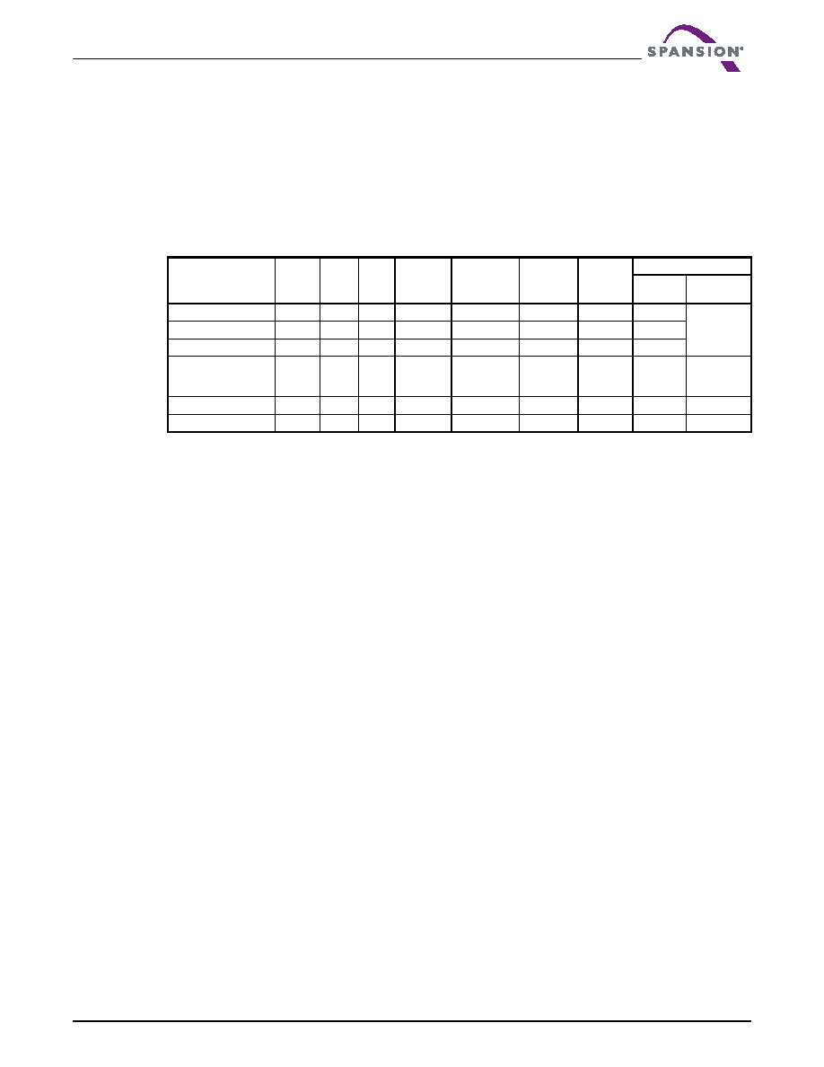
Table 7.1 Device Bus Operations
Operation
CE#
OE#
WE#
RESET#
WP#/ACC
Addresses
DQ0–
DQ7
DQ8–DQ15
BYTE#
= VIH
BYTE#
= VIL
Read
L
H
X
AIN
DOUT
DQ8–DQ14
= High-Z,
DQ15 = A-1
Write (Program/Erase)
L
H
L
H
AIN
Accelerated Program
L
H
L
H
VHH
AIN
Standby
VCC
<Helv>±
0.3 V
XX
VCC
<Helv>±
0.3 V
H
X
High-Z
Output Disable
L
H
X
High-Z
Reset
X
L
X
High-Z
相关PDF资料 |
PDF描述 |
|---|---|
| S29GL256N10FFI010 | MirrorBit Flash Family |
| S29GL256N80FAI010 | MirrorBit Flash Family |
| S29GL256N80FFI010 | MirrorBit Flash Family |
| S29GL256N80FFI013 | MirrorBit Flash Family |
| S29JL032H90TAI223 | 2M X 16 FLASH 3V PROM, 90 ns, PDSO48 |
相关代理商/技术参数 |
参数描述 |
|---|---|
| S29GL256N10FAI020 | 制造商:Spansion 功能描述: |
| S29GL256N10FFI010 | 制造商:Spansion 功能描述:NOR Flash Parallel 3V/3.3V 256Mbit 32M/16M x 8bit/16bit 100ns 64-Pin Fortified BGA Tray 制造商:Spansion 功能描述:MIRRORBIT FLASH 256MB SMD 29LV256 |
| S29GL256N10FFI012 | 制造商:Spansion 功能描述:Flash - NOR IC |
| S29GL256N10FFI020 | 制造商:Spansion 功能描述:NOR Flash Parallel 3V/3.3V 256Mbit 32M/16M x 8bit/16bit 100ns 64-Pin Fortified BGA Tray 制造商:Spansion 功能描述:MIRRORBIT FLASH 256MB SMD 29LV256 |
| S29GL256N10TFI010 | 功能描述:IC FLASH 制造商:cypress semiconductor corp 系列:GL-N 包装:托盘 零件状态:在售 存储器类型:非易失 存储器格式:闪存 技术:FLASH - NOR 存储容量:256Mb (32M x 8,16M x 16) 写周期时间 - 字,页:100ns 访问时间:100ns 存储器接口:并联 电压 - 电源:2.7 V ~ 3.6 V 工作温度:-40°C ~ 85°C(TA) 安装类型:表面贴装 封装/外壳:56-TFSOP(0.724",18.40mm 宽) 供应商器件封装:56-TSOP 标准包装:91 |
发布紧急采购,3分钟左右您将得到回复。