- 您现在的位置:买卖IC网 > PDF目录225141 > S29JL032H90TAI223 (ADVANCED MICRO DEVICES INC) 2M X 16 FLASH 3V PROM, 90 ns, PDSO48 PDF资料下载
参数资料
| 型号: | S29JL032H90TAI223 |
| 厂商: | ADVANCED MICRO DEVICES INC |
| 元件分类: | PROM |
| 英文描述: | 2M X 16 FLASH 3V PROM, 90 ns, PDSO48 |
| 封装: | MO-142DD, TSOP-48 |
| 文件页数: | 5/66页 |
| 文件大小: | 1691K |
| 代理商: | S29JL032H90TAI223 |
第1页第2页第3页第4页当前第5页第6页第7页第8页第9页第10页第11页第12页第13页第14页第15页第16页第17页第18页第19页第20页第21页第22页第23页第24页第25页第26页第27页第28页第29页第30页第31页第32页第33页第34页第35页第36页第37页第38页第39页第40页第41页第42页第43页第44页第45页第46页第47页第48页第49页第50页第51页第52页第53页第54页第55页第56页第57页第58页第59页第60页第61页第62页第63页第64页第65页第66页
March 10, 2005 S29JL032H_00A11
S29JL032H
11
Ad vance
Info rmat i o n
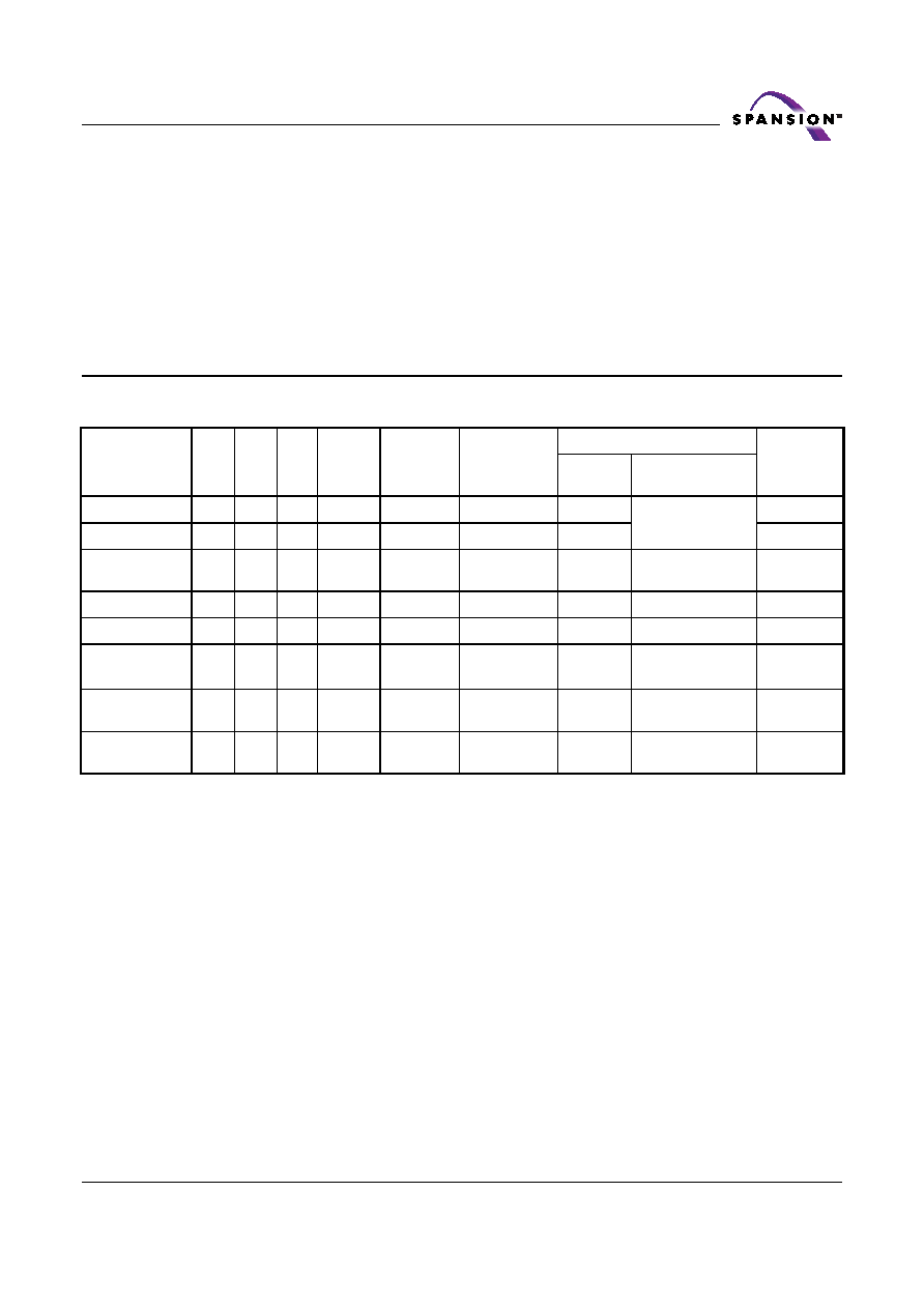
Device Bus Operations
This section describes the requirements and use of the device bus operations,
which are initiated through the internal command register. The command register
itself does not occupy any addressable memory location. The register is a latch
used to store the commands, along with the address and data information
needed to execute the command. The contents of the register serve as inputs to
the internal state machine. The state machine outputs dictate the function of the
device. Table 1 lists the device bus operations, the inputs and control levels they
require, and the resulting output. The following subsections describe each of
these operations in further detail.
Table 1. S29JL032H Device Bus Operations
Legend: L = Logic Low = VIL, H = Logic High = VIH, VID = 11.5–12.5 V, VHH = 9.0 ± 0.5 V, X = Don’t Care, SA = Sector
Address, AIN = Address In, DIN = Data In, DOUT = Data Out
Notes:
1. Addresses are A20:A0 in word mode (BYTE# = VIH), A20:A-1 in byte mode (BYTE# = VIL).
2. The sector protect and sector unprotect functions may also be implemented via programming equipment. See
the “Sector/Sector Block Protection and Unprotection” section.
3. If WP#/ACC = VIL, the two outermost boot sectors remain protected. If WP#/ACC = VIH, protection on the two out-
ermost boot sectors depends on whether they were last protected or unprotected using the method described in
“Sector/Sector Block Protection and Unprotection”. If WP#/ACC = VHH, all sectors will be unprotected.
Operation
CE#
OE# WE# RESET# WP#/ACC
Addresses
DQ15–DQ8
DQ7–DQ0
BYTE# =
VIH
BYTE# = VIL
Read
L
H
L/H
AIN
DOUT
DQ14–DQ8 = High-
Z, DQ15 = A-1
DOUT
Write
L
H
L
H
AIN
DIN
Standby
VCC ±
0.3 V
X
VCC ±
0.3 V
L/H
X
High-Z
Output Disable
L
H
L/H
X
High-Z
Reset
X
L
L/H
X
High-Z
Sector Protect
L
H
L
VID
L/H
SA, A6 = L,
A1 = H, A0 = L
X
DIN
Sector Unprotect
L
H
L
VID
SA, A6 = H,
A1 = H, A0 = L
X
DIN
Temporary
Sector Unprotect
X
VID
AIN
DIN
High-Z
DIN
相关PDF资料 |
PDF描述 |
|---|---|
| S29WS064N0PBAW011 | 256/128/64 MEGABIT CMOS 1.8 VOLT ONLY SIMULTANEOUS READ/WRITE BURST MODE FLASH MEMORY |
| S29WS128N0LBFI111 | 256/128/64 MEGABIT CMOS 1.8 VOLT ONLY SIMULTANEOUS READ/WRITE BURST MODE FLASH MEMORY |
| S29WS128N0LBFI112 | 256/128/64 MEGABIT CMOS 1.8 VOLT ONLY SIMULTANEOUS READ/WRITE BURST MODE FLASH MEMORY |
| S29WS128N0LBFI113 | 256/128/64 MEGABIT CMOS 1.8 VOLT ONLY SIMULTANEOUS READ/WRITE BURST MODE FLASH MEMORY |
| S29WS128N0LBFW011 | Test Clip; Current Rating:100A; Body Material:Steel; Features:Unmarked; Jaw Opening Max:1.625"; Overall Length:6" RoHS Compliant: NA |
相关代理商/技术参数 |
参数描述 |
|---|---|
| S29JL032H90TAI310 | 功能描述:闪存 3V 32Mb Float Gate top boot 2Banks 90s RoHS:否 制造商:ON Semiconductor 数据总线宽度:1 bit 存储类型:Flash 存储容量:2 MB 结构:256 K x 8 定时类型: 接口类型:SPI 访问时间: 电源电压-最大:3.6 V 电源电压-最小:2.3 V 最大工作电流:15 mA 工作温度:- 40 C to + 85 C 安装风格:SMD/SMT 封装 / 箱体: 封装:Reel |
| S29JL032H90TAI311 | 制造商:SPANSION 制造商全称:SPANSION 功能描述:32M BIT CMOS 3.0V FLASH MEMORY |
| S29JL032H90TAI312 | 制造商:SPANSION 制造商全称:SPANSION 功能描述:32M BIT CMOS 3.0V FLASH MEMORY |
| S29JL032H90TAI313 | 功能描述:闪存 3V 32M SIMULTANEOUS READ/WRITE FLASH RoHS:否 制造商:ON Semiconductor 数据总线宽度:1 bit 存储类型:Flash 存储容量:2 MB 结构:256 K x 8 定时类型: 接口类型:SPI 访问时间: 电源电压-最大:3.6 V 电源电压-最小:2.3 V 最大工作电流:15 mA 工作温度:- 40 C to + 85 C 安装风格:SMD/SMT 封装 / 箱体: 封装:Reel |
| S29JL032H90TAI320 | 功能描述:闪存 3V 32Mb Float Gate btm boot 2Banks 90s RoHS:否 制造商:ON Semiconductor 数据总线宽度:1 bit 存储类型:Flash 存储容量:2 MB 结构:256 K x 8 定时类型: 接口类型:SPI 访问时间: 电源电压-最大:3.6 V 电源电压-最小:2.3 V 最大工作电流:15 mA 工作温度:- 40 C to + 85 C 安装风格:SMD/SMT 封装 / 箱体: 封装:Reel |
发布紧急采购,3分钟左右您将得到回复。