参数资料
| 型号: | SA5230NG |
| 厂商: | ON Semiconductor |
| 文件页数: | 18/18页 |
| 文件大小: | 0K |
| 描述: | IC OPAMP LOW VOLTAGE 8-DIP |
| 标准包装: | 50 |
| 放大器类型: | 通用 |
| 电路数: | 1 |
| 输出类型: | 满摆幅 |
| 转换速率: | 0.25 V/µs |
| 增益带宽积: | 600kHz |
| 电流 - 输入偏压: | 40nA |
| 电压 - 输入偏移: | 400µV |
| 电流 - 电源: | 1.1mA |
| 电流 - 输出 / 通道: | 32mA |
| 电压 - 电源,单路/双路(±): | 1.8 V ~ 15 V,±0.9 V ~ 7.5 V |
| 工作温度: | -40°C ~ 85°C |
| 安装类型: | 通孔 |
| 封装/外壳: | 8-DIP(0.300",7.62mm) |
| 供应商设备封装: | 8-PDIP |
| 包装: | 管件 |
NE5230, SA5230, SE5230
http://onsemi.com
9
The full output power bandwidth range for VCC equals
2.0 V, is above 40 kHz for the maximum bias current setting
and greater than 10 kHz at the minimum bias current setting.
If extremely low signal distortion (<0.05%) is required at
low supply voltages, exclude the commonmode crossover
point (VB1) from the commonmode signal range. This can
be accomplished by proper bias selection or by using an
inverting amplifier configuration.
Most single supply designs necessitate that the inputs to
the op amp be biased between VCC and ground. This is to
assure that the input signal swing is within the working
commonmode range of the amplifier. This leads to another
helpful and unique property of the NE5230 that other CMOS
and bipolar low voltage parts cannot achieve. It is the simple
fact that the input commonmode voltage can go beyond
either the positive or negative supply voltages. This benefit
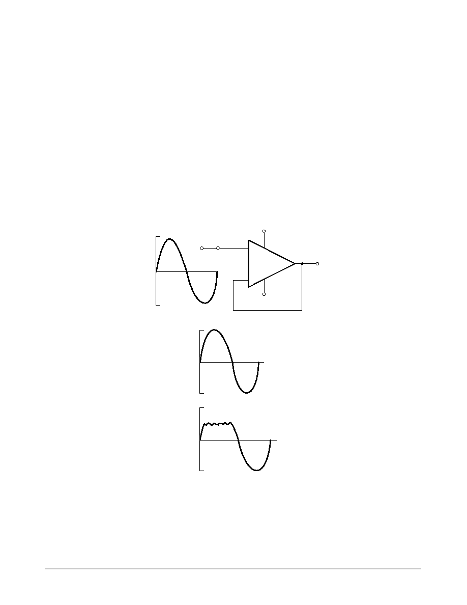
is made very clear in a noninverting voltagefollower
configuration. This is shown in Figure 5 where the input sine
wave allows an undistorted output sine wave which will
swing less than 100 mV of either supply voltage. Many
competitive parts will show severe clipping caused by input
commonmode limitations. The NE5230 in this
configuration offers more freedom for quiescent biasing of
the inputs close to the positive supply rail where similar op
amps would not allow signal processing.
There are not as many considerations when designing
with the NE5230 as with other devices. Since the NE5230
is internallycompensated and has a unity gainbandwidth
of 600 kHz, board layout is not so stringent as for very high
frequency devices such as the NE5205. The output
capability of the NE5230 allows it to drive relatively high
capacitive loads and small resistive loads. The power supply
pins should be decoupled with a lowpass RC network as
close to the supply pins as possible to eliminate 60 Hz and
other external power line noise, although the power supply
rejection ratio (PSRR) for the part is very high. The pinout
for the NE5230 is the same as the standard single op amp
pinout with the exception of the bias current adjusting pin.
V+
V
+
NE5230
OTHER
PARTS
V+
V
V+
V
V+
V
Figure 5. In a noninverting voltagefollower configuration, the NE5230 will give full railtorail swing.
Other low voltage amplifiers will not because they are limited by their input commonmode
range and output swing capability.
相关PDF资料 |
PDF描述 |
|---|---|
| M80-8280822 | CONN HDR 2MM W/LATCH 8POS SMD |
| M80-8261422 | CONN HDR 2MM VERT 14POS SMD |
| SA18CA | TVS BIDIRECT 500W 18V DO-15 |
| SZP6SMB62CAT3G | TVS ZENER 600W 62V BIDIR SMB |
| 961238-6300-AR-PR | CONN HEADER STR DL 38PS GOLD SMD |
相关代理商/技术参数 |
参数描述 |
|---|---|
| SA5232 | 制造商:PHILIPS 制造商全称:NXP Semiconductors 功能描述:Matched dual high-performance low-voltage operational amplifier |
| SA5232D | 制造商:PHILIPS 制造商全称:NXP Semiconductors 功能描述:Matched dual high-performance low-voltage operational amplifier |
| SA5232D,112 | 功能描述:运算放大器 - 运放 MATCHED DUAL LOW-VOLT OP AMP RoHS:否 制造商:STMicroelectronics 通道数量:4 共模抑制比(最小值):63 dB 输入补偿电压:1 mV 输入偏流(最大值):10 pA 工作电源电压:2.7 V to 5.5 V 安装风格:SMD/SMT 封装 / 箱体:QFN-16 转换速度:0.89 V/us 关闭:No 输出电流:55 mA 最大工作温度:+ 125 C 封装:Reel |
| SA5232D,118 | 功能描述:运算放大器 - 运放 MATCHED DUAL LOW-VOLT OP AMP RoHS:否 制造商:STMicroelectronics 通道数量:4 共模抑制比(最小值):63 dB 输入补偿电压:1 mV 输入偏流(最大值):10 pA 工作电源电压:2.7 V to 5.5 V 安装风格:SMD/SMT 封装 / 箱体:QFN-16 转换速度:0.89 V/us 关闭:No 输出电流:55 mA 最大工作温度:+ 125 C 封装:Reel |
| SA5232D/01 | 功能描述:运算放大器 - 运放 DUAL LVOP AMP -40-85 RoHS:否 制造商:STMicroelectronics 通道数量:4 共模抑制比(最小值):63 dB 输入补偿电压:1 mV 输入偏流(最大值):10 pA 工作电源电压:2.7 V to 5.5 V 安装风格:SMD/SMT 封装 / 箱体:QFN-16 转换速度:0.89 V/us 关闭:No 输出电流:55 mA 最大工作温度:+ 125 C 封装:Reel |
发布紧急采购,3分钟左右您将得到回复。