- 您现在的位置:买卖IC网 > PDF目录10243 > SA571DR2G (ON Semiconductor)IC COMPANDOR DUAL GAIN 16-SOIC PDF资料下载
参数资料
| 型号: | SA571DR2G |
| 厂商: | ON Semiconductor |
| 文件页数: | 10/11页 |
| 文件大小: | 0K |
| 描述: | IC COMPANDOR DUAL GAIN 16-SOIC |
| 标准包装: | 1 |
| 类型: | 压缩扩展器 |
| 应用: | 蜂窝式无线电,播放器 |
| 安装类型: | 表面贴装 |
| 封装/外壳: | 16-SOIC(0.295",7.50mm 宽) |
| 供应商设备封装: | 16-SOIC W |
| 包装: | 标准包装 |
| 其它名称: | SA571DR2GOSDKR |
SA571
http://onsemi.com
8
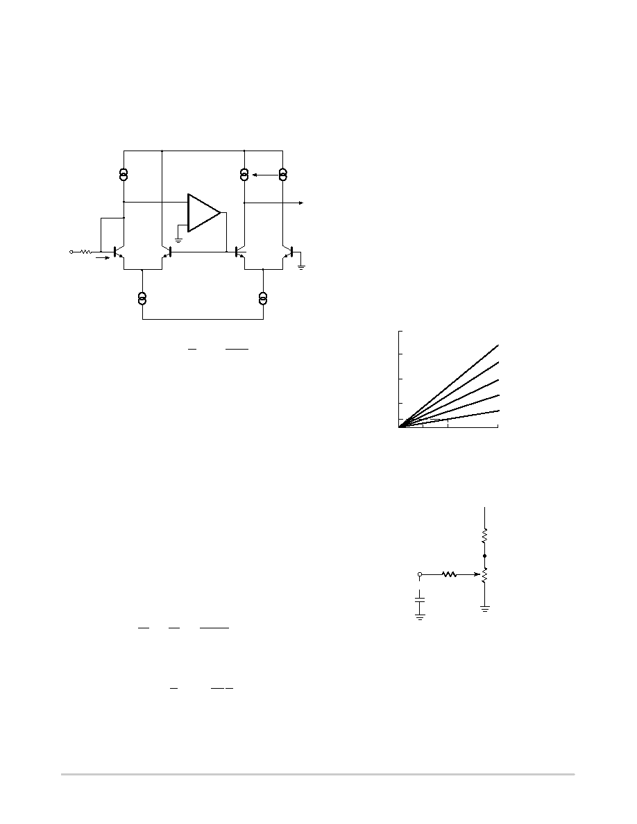
Variable Gain Cell
Figure 12 is a diagram of the variable gain cell. This is a
linearized twoquadrant transconductance multiplier. Q1,
Q2 and the op amp provide a predistorted drive signal for the
gain control pair, Q3 and Q4. The gain is controlled by IG and
a current mirror provides the output current.
Q1
Q2
Q3
Q4
NOTE:
I2 (= 2I1)
280
mA
IG
IIN
VIN
R2
20k
I1
140
mA
V+
V
I
OUT +
I
G
I
1
I
IN +
I
G VIN
I
2 R2
Figure 12. Simplified
DG Cell Schematic
+
The op amp maintains the base and collector of Q1 at
ground potential (VREF) by controlling the base of Q2. The
input current IIN (= VIN/R2) is thus forced to flow through
Q1 along with the current I1, so IC1 = I1 + IIN. Since I2 has
been set at twice the value of I1, the current through Q2 is:
I2 (I1 + IIN) = I1 IIN = IC2.
The op amp has thus forced a linear current swing between
Q1 and Q2 by providing the proper drive to the base of Q2.
This drive signal will be linear for small signals, but very
nonlinear for large signals, since it is compensating for the
nonlinearity of the differential pair, Q1 and Q2, under large
signal conditions.
The key to the circuit is that this same predistorted drive
signal is applied to the gain control pair, Q3 and Q4. When
two differential pairs of transistors have the same signal
applied, their collector current ratios will be identical
regardless of the magnitude of the currents. This gives us:
I
C1
I
C2
+
I
C4
I
C3
+
I
1 ) IIN
I
1 * IIN
plus the relationships IG = IC3 + IC4 and IOUT = IC4 IC3 will
yield the multiplier transfer function,
I
OUT +
I
G
I
1
I
IN +
V
IN
R
2
I
G
I
1
This equation is linear and temperatureinsensitive, but it
assumes ideal transistors.
If the transistors are not perfectly matched, a parabolic,
nonlinearity is generated, which results in second
harmonic distortion. Figure 13 gives an indication of the
magnitude of the distortion caused by a given input level and
offset voltage. The distortion is linearly proportional to the
magnitude of the offset and the input level. Saturation of the
gain cell occurs at a +8 dBm level. At a nominal operating
level of 0 dBm, a 1.0 mV offset will yield 0.34% of second
harmonic distortion. Most circuits are somewhat better than
this, which means our overall offsets are typically about mV.
The distortion is not affected by the magnitude of the gain
control current, and it does not increase as the gain is
changed. This second harmonic distortion could be
eliminated by making perfect transistors, but since that
would be difficult, we have had to resort to other methods.
A trim pin has been provided to allow trimming of the
internal offsets to zero, which effectively eliminated second
harmonic distortion. Figure 14 shows the simple trim
network required.
4
3
2
1
.34
6
0
+6
4mV
3mV
2mV
1mV
INPUT LEVEL (dBm)
%
THD
Figure 13.
DG Cell Distortion vs. Offset Voltage
3.6V
VCC
R
6.2k
W
To THD Trim
≈200pF
Figure 14. THD Trim Network
20k
W
相关PDF资料 |
PDF描述 |
|---|---|
| VI-26T-MY | CONVERTER MOD DC/DC 6.5V 50W |
| SA575DTBR2G | IC COMPANDOR 2CHAN GAIN 20-TSSOP |
| VE-B2P-MW-F1 | CONVERTER MOD DC/DC 13.8V 100W |
| VE-B31-IV-S | CONVERTER MOD DC/DC 12V 150W |
| VI-26H-MY | CONVERTER MOD DC/DC 52V 50W |
相关代理商/技术参数 |
参数描述 |
|---|---|
| SA571E-2200 | 制造商:Elan 功能描述:TOUCH PAD |
| SA571FB | 制造商:SIGNET 功能描述: |
| SA571N | 功能描述:音频放大器 Dual Gain Compandor RoHS:否 制造商:STMicroelectronics 产品:General Purpose Audio Amplifiers 输出类型:Digital 输出功率: THD + 噪声: 工作电源电压:3.3 V 电源电流: 最大功率耗散: 最大工作温度: 安装风格:SMD/SMT 封装 / 箱体:TQFP-64 封装:Reel |
| SA571N,602 | 制造商:NXP Semiconductors 功能描述: |
| SA571NG | 功能描述:音频放大器 Dual Gain Compandor Industrial Temp RoHS:否 制造商:STMicroelectronics 产品:General Purpose Audio Amplifiers 输出类型:Digital 输出功率: THD + 噪声: 工作电源电压:3.3 V 电源电流: 最大功率耗散: 最大工作温度: 安装风格:SMD/SMT 封装 / 箱体:TQFP-64 封装:Reel |
发布紧急采购,3分钟左右您将得到回复。