- 您现在的位置:买卖IC网 > PDF目录10243 > SA571DR2G (ON Semiconductor)IC COMPANDOR DUAL GAIN 16-SOIC PDF资料下载
参数资料
| 型号: | SA571DR2G |
| 厂商: | ON Semiconductor |
| 文件页数: | 9/11页 |
| 文件大小: | 0K |
| 描述: | IC COMPANDOR DUAL GAIN 16-SOIC |
| 标准包装: | 1 |
| 类型: | 压缩扩展器 |
| 应用: | 蜂窝式无线电,播放器 |
| 安装类型: | 表面贴装 |
| 封装/外壳: | 16-SOIC(0.295",7.50mm 宽) |
| 供应商设备封装: | 16-SOIC W |
| 包装: | 标准包装 |
| 其它名称: | SA571DR2GOSDKR |
SA571
http://onsemi.com
7
Figure 9 shows the rectifier circuit in more detail. The op
amp is a onestage op amp, biased so that only one output
device is on at a time. The noninverting input, (the base of
Q1), which is shown grounded, is actually tied to the internal
1.8 V, VREF. The inverting input is tied to the op amp output,
(the emitters of Q5 and Q6), and the input summing resistor
R1. The single diode between the bases of Q5 and Q6 assures
that only one device is on at a time. To detect the output
current of the op amp, we simply use the collector currents
of the output devices Q5 and Q6. Q6 will conduct when the
input swings positive and Q5 conducts when the input
swings negative. The collector currents will be in error by
the
a of Q5 or Q6 on negative or positive signal swings,
respectively. ICs such as this have typical NPN
b’s of 200
and PNP
b’s of 40. The a’s of 0.995 and 0.975 will produce
errors of 0.5% on negative swings and 2.5% on positive
swings. The 1.5% average of these errors yields a mere 0.13
dB gain error.
V+
Q1 Q2
Q3
Q4
Q7
Q5
Q6
Q8
Q9
CR
D1
I1
I2
VIN
V
I
G + 2
V
IN avg
R1
NOTE:
Figure 9. Simplified Rectifier Schematic
R1
10k
W
RS
10k
W
At very low input signal levels the bias current of Q2,
(typically 50 nA), will become significant as it must be
supplied by Q5. Another low level error can be caused by DC
coupling into the rectifier. If an offset voltage exists between
the VIN input pin and the base of Q2, an error current of
VOS/R1 will be generated. A mere 1.0 mV of offset will
cause an input current of 100 nA which will produce twice
the error of the input bias current. For highest accuracy, the
rectifier should be coupled capacitively. At high input levels
the
b of the PNP Q6 will begin to suffer, and there will be an
increasing error until the circuit saturates. Saturation can be
avoided by limiting the current into the rectifier input to
250
mA. If necessary, an external resistor may be placed in
shows the rectifier accuracy vs. input level at a frequency of
1.0 kHz.
ERROR
GAIN
dB
+1
0
1
40
20
0
RECTIFIER INPUT dBm
Figure 10. Rectifier Accuracy
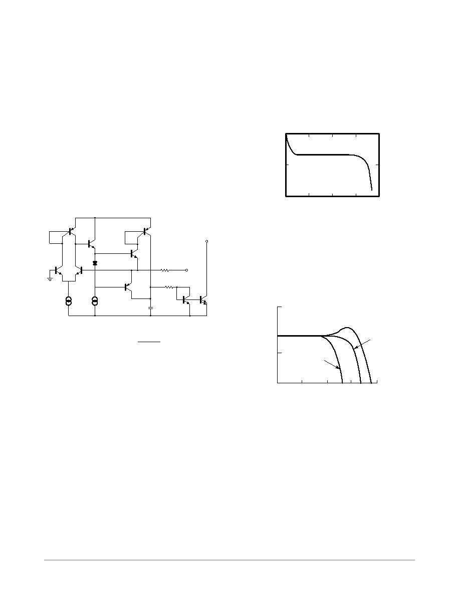
At very high frequencies, the response of the rectifier will
fall off. The rolloff will be more pronounced at lower input
levels due to the increasing amount of gain required to
switch between Q5 or Q6 conducting. The rectifier
frequency response for input levels of 0 dBm, 20 dBm, and
40 dBm is shown in Figure 11. The response at all three
levels is flat to well above the audio range.
0
3
10k
1MEG
INPUT = 0dBm
20dBm
40dBm
FREQUENCY (Hz)
GAIN
ERROR
(dB)
Figure 11. Rectifier Frequency Response vs.
Input Level
相关PDF资料 |
PDF描述 |
|---|---|
| VI-26T-MY | CONVERTER MOD DC/DC 6.5V 50W |
| SA575DTBR2G | IC COMPANDOR 2CHAN GAIN 20-TSSOP |
| VE-B2P-MW-F1 | CONVERTER MOD DC/DC 13.8V 100W |
| VE-B31-IV-S | CONVERTER MOD DC/DC 12V 150W |
| VI-26H-MY | CONVERTER MOD DC/DC 52V 50W |
相关代理商/技术参数 |
参数描述 |
|---|---|
| SA571E-2200 | 制造商:Elan 功能描述:TOUCH PAD |
| SA571FB | 制造商:SIGNET 功能描述: |
| SA571N | 功能描述:音频放大器 Dual Gain Compandor RoHS:否 制造商:STMicroelectronics 产品:General Purpose Audio Amplifiers 输出类型:Digital 输出功率: THD + 噪声: 工作电源电压:3.3 V 电源电流: 最大功率耗散: 最大工作温度: 安装风格:SMD/SMT 封装 / 箱体:TQFP-64 封装:Reel |
| SA571N,602 | 制造商:NXP Semiconductors 功能描述: |
| SA571NG | 功能描述:音频放大器 Dual Gain Compandor Industrial Temp RoHS:否 制造商:STMicroelectronics 产品:General Purpose Audio Amplifiers 输出类型:Digital 输出功率: THD + 噪声: 工作电源电压:3.3 V 电源电流: 最大功率耗散: 最大工作温度: 安装风格:SMD/SMT 封装 / 箱体:TQFP-64 封装:Reel |
发布紧急采购,3分钟左右您将得到回复。