- 您现在的位置:买卖IC网 > PDF目录69331 > SAB-XC164CM-4F40F (INFINEON TECHNOLOGIES AG) 16-BIT, FLASH, 40 MHz, MICROCONTROLLER, PQFP64 PDF资料下载
参数资料
| 型号: | SAB-XC164CM-4F40F |
| 厂商: | INFINEON TECHNOLOGIES AG |
| 元件分类: | 微控制器/微处理器 |
| 英文描述: | 16-BIT, FLASH, 40 MHz, MICROCONTROLLER, PQFP64 |
| 封装: | PLASTIC, TQFP-64 |
| 文件页数: | 51/69页 |
| 文件大小: | 1591K |
| 代理商: | SAB-XC164CM-4F40F |
第1页第2页第3页第4页第5页第6页第7页第8页第9页第10页第11页第12页第13页第14页第15页第16页第17页第18页第19页第20页第21页第22页第23页第24页第25页第26页第27页第28页第29页第30页第31页第32页第33页第34页第35页第36页第37页第38页第39页第40页第41页第42页第43页第44页第45页第46页第47页第48页第49页第50页当前第51页第52页第53页第54页第55页第56页第57页第58页第59页第60页第61页第62页第63页第64页第65页第66页第67页第68页第69页
XC164CM
Derivatives
Electrical Parameters
Data Sheet
53
V1.2, 2006-03
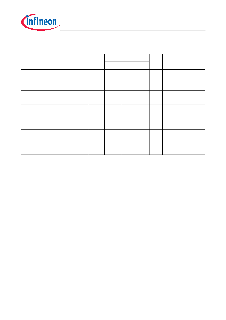
Table 13
Power Consumption XC164CM (Operating Conditions apply)
Parameter
Sym-
bol
Limit Values
Unit Test Condition
Min.
Max.
Power supply current (active)
with all peripherals active
I
DDI
–
10 +
2.6
× f
CPU
mA
f
CPU in [MHz]
1)2)
1) During Flash programming or erase operations the supply current is increased by max. 5 mA.
2) The supply current is a function of the operating frequency. This dependency is illustrated in Figure 11.
These parameters are tested at
VDDImax and maximum CPU clock frequency with all outputs disconnected and
all inputs at
VIL or VIH.
Pad supply current
I
DDP
–5
mA
3)
3) The pad supply voltage pins (
VDDP) mainly provides the current consumed by the pin output drivers. A small
amount of current is consumed even though no outputs are driven, because the drivers’ input stages are
switched and also the Flash module draws some power from the
VDDP supply.
Idle mode supply current with
all peripherals active
I
IDX
–
10 +
1.2
× f
CPU
mA
f
CPU in [MHz]
Sleep and Power down mode
supply current caused by
leakage4)
4) The total supply current in Sleep and Power down mode is the sum of the temperature dependent leakage
current and the frequency dependent current for RTC and main oscillator.
I
PDL
5)
5) This parameter is determined mainly by the transistor leakage currents. This current heavily depends on the
junction temperature (see Figure 13). The junction temperature
TJ is the same as the ambient temperature TA
if no current flows through the port output drivers. Otherwise, the resulting temperature difference must be
taken into account.
–
128,000
× e-α
mA
V
DDI = VDDImax
6)
T
J in [°C]
α =
4670 / (273 +
T
J)
6) All inputs (including pins configured as inputs) at 0 V to 0.1 V or at
VDDP - 0.1 V to VDDP, all outputs (including
pins configured as outputs) disconnected. This parameter is tested at 25
°C and is valid for T
J ≥ 25 °C.
Sleep and Power down mode
supply current caused by
leakage and the RTC running,
clocked by the main oscillator4)
I
PDM
7)
7) This parameter is determined mainly by the current consumed by the oscillator switched to low gain mode (see
Figure 12). This current, however, is influenced by the external oscillator circuitry (crystal, capacitors). The
given values refer to a typical circuitry and may change in case of a not optimized external oscillator circuitry.
–
0.6 +
0.02
× f
OSC
+
I
PDL
mA
V
DDI = VDDImax
f
OSC in [MHz]
相关PDF资料 |
PDF描述 |
|---|---|
| SAB-XC164CM-8F20F | 16-BIT, FLASH, 20 MHz, MICROCONTROLLER, PQFP64 |
| SAB-XC164KM-4F40F | 16-BIT, FLASH, 40 MHz, MICROCONTROLLER, PQFP64 |
| SAB-XC164KM-4F20F | 16-BIT, FLASH, 20 MHz, MICROCONTROLLER, PQFP64 |
| SAK-XC164KM-4F40F | 16-BIT, FLASH, 40 MHz, MICROCONTROLLER, PQFP64 |
| SAB-XC164TM-8F20F | 16-BIT, FLASH, 20 MHz, MICROCONTROLLER, PQFP64 |
相关代理商/技术参数 |
参数描述 |
|---|---|
| SAB-XC167CI-16F20F | 制造商:INFINEON 制造商全称:Infineon Technologies AG 功能描述:16-Bi t Single-Chip Microcontroller Preliminary |
| SAB-XC167CI-16F40F | 制造商:INFINEON 制造商全称:Infineon Technologies AG 功能描述:16-Bi t Single-Chip Microcontroller Preliminary |
| SAC | 制造商:TSC 制造商全称:Taiwan Semiconductor Company, Ltd 功能描述:Low Capacitance Transient Voltage Suppressor Diodes |
| SAC 8250 | 制造商:Edsyn International 功能描述:Bulk |
| SAC+0107 | 制造商:AIM Metals & Alloys LP 功能描述:Solder Bar-2.5lbs. 制造商:AIM PRODUCTS LLC. 功能描述:Solder Bar-2.5lbs. |
发布紧急采购,3分钟左右您将得到回复。