- 您现在的位置:买卖IC网 > PDF目录11813 > SC16C2550IB48,128 (NXP Semiconductors)IC DUART SOT313-2 PDF资料下载
参数资料
| 型号: | SC16C2550IB48,128 |
| 厂商: | NXP Semiconductors |
| 文件页数: | 44/46页 |
| 文件大小: | 0K |
| 描述: | IC DUART SOT313-2 |
| 标准包装: | 2,000 |
| 特点: | 2 通道 |
| 通道数: | 2,DUART |
| FIFO's: | 16 字节 |
| 电源电压: | 2.5V,3.3V,5V |
| 带自动流量控制功能: | 是 |
| 带IrDA 编码器/解码器: | 是 |
| 带故障启动位检测功能: | 是 |
| 带调制解调器控制功能: | 是 |
| 带CMOS: | 是 |
| 安装类型: | 表面贴装 |
| 封装/外壳: | 48-LQFP |
| 供应商设备封装: | 48-LQFP(7x7) |
| 包装: | 管件 |
| 其它名称: | 935270020128 SC16C2550IB48-T SC16C2550IB48-T-ND |
第1页第2页第3页第4页第5页第6页第7页第8页第9页第10页第11页第12页第13页第14页第15页第16页第17页第18页第19页第20页第21页第22页第23页第24页第25页第26页第27页第28页第29页第30页第31页第32页第33页第34页第35页第36页第37页第38页第39页第40页第41页第42页第43页当前第44页第45页第46页
Philips Semiconductors
SC16C2550
Dual UART with 16 bytes of transmit and receive FIFOs and IrDA
encoder/decoder
Product data
Rev. 03 — 19 June 2003
7 of 46
9397 750 11621
Koninklijke Philips Electronics N.V. 2003. All rights reserved.
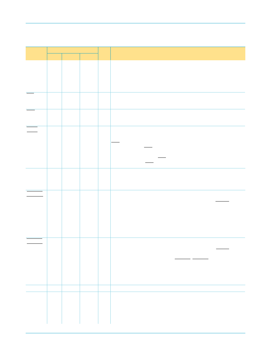
INTA,
INTB
30, 29 33, 32
30, 29
O
Interrupt A, B (3-State). This function is associated with individual channel
interrupts, INTA, INTB. INTA, INTB are enabled when MCR bit 3 is set to a
logic 1, interrupts are enabled in the interrupt enable register (IER), and is
active when an interrupt condition exists. Interrupt conditions include:
receiver errors, available receiver buffer data, transmit buffer empty, or
when a modem status ag is detected.
IOR
21
24
19
I
Read strobe (Active-LOW strobe). A logic 0 transition on this pin will load
the contents of an internal register dened by address bits A0-A2 onto the
SC16C2550 data bus (D0-D7) for access by external CPU.
IOW18
20
15
I
Write strobe (Active-LOW strobe). A logic 0 transition on this pin will
transfer the contents of the data bus (D0-D7) from the external CPU to an
internal register that is dened by address bits A0-A2.
OP2A,
OP2B
31, 13 35, 15
32, 9
O
Output 2 (user-dened). This function is associated with individual
channels, A through B. The state at these pin(s) are dened by the user
and through MCR register bit 3. INTA, INTB are set to the active mode and
OP2 to logic 0 when MCR[3] is set to a logic 1. INTA, INTB are set to the
3-State mode and OP2 to a logic 1 when MCR[3] is set to a logic 0. See
bit 3, Modem Control Register (MCR[3]). Since these bits control both the
INTA, INTB operation and OP2 outputs, only one function should be used
at one time, INT or OP2.
RESET
35
39
36
I
Reset (Active-HIGH). A logic 1 on this pin will reset the internal registers
and all the outputs. The UART transmitter output and the receiver input will
be disabled during reset time. (See Section 7.11 “SC16C2550 external
reset condition” for initialization details.)
RXRDYA,
RXRDYB
-
34, 23
31, 18
O
Receive Ready A, B (Active-LOW). This function is associated with
PLCC44 and LQFP48 packages only. This function provides the
RX FIFO/RHR status for individual receive channels (A-B). RXRDYn is
primarily intended for monitoring DMA mode 1 transfers for the receive data
FIFOs. A logic 0 indicates there is a receive data to read/upload, i.e.,
receive ready status with one or more RX characters available in the
FIFO/RHR. This pin is a logic 1 when the FIFO/RHR is empty or when the
programmed trigger level has not been reached. This signal can also be
used for single mode transfers (DMA mode 0).
TXRDYA,
TXRDYB
-
1, 12
43, 6
O
Transmit Ready A, B (Active-LOW). This function is associated with
PLCC44 and LQFP48 packages only. These outputs provide the
TX FIFO/THR status for individual transmit channels (A-B). TXRDYn is
primarily intended for monitoring DMA mode 1 transfers for the transmit
data FIFOs. An individual channel’s TXRDYA, TXRDYB buffer ready status
is indicated by logic 0, i.e., at lease one location is empty and available in
the FIFO or THR. This pin goes to a logic 1 (DMA mode 1) when there are
no more empty locations in the FIFO or THR. This signal can also be used
for single mode transfers (DMA mode 0).
VCC
40
44
42
I
Power supply input.
XTAL1
16
18
13
I
Crystal or external clock input. Functions as a crystal input or as an
external clock input. A crystal can be connected between this pin and
XTAL2 to form an internal oscillator circuit. This conguration requires an
external 1 M
resistor between the XTAL1 and XTAL2 pins. Alternatively,
an external clock can be connected to this pin to provide custom data rates.
Table 2:
Pin description…continued
Symbol
Pin
Type Description
DIP40 PLCC44 LQFP48
相关PDF资料 |
PDF描述 |
|---|---|
| SC16C2550IB48,157 | IC DUART SOT313-2 |
| SC16C2550IA44,518 | IC DUART SOT187-2 |
| SC16C2550IA44,512 | IC DUART SOT187-2 |
| VI-B7N-IX-F1 | CONVERTER MOD DC/DC 18.5V 75W |
| SC16C2550BIN40,112 | IC UART DUAL W/FIFO 40-DIP |
相关代理商/技术参数 |
参数描述 |
|---|---|
| SC16C2550IN40 | 制造商:PHILIP 功能描述: |
| SC16C2550IN40,112 | 功能描述:IC UART DUAL W/FIFO 40-DIP RoHS:是 类别:集成电路 (IC) >> 接口 - UART(通用异步接收器/发送器) 系列:- 标准包装:250 系列:- 特点:* 通道数:2,DUART FIFO's:16 字节 规程:RS232,RS485 电源电压:2.25 V ~ 5.5 V 带并行端口:- 带自动流量控制功能:是 带IrDA 编码器/解码器:是 带故障启动位检测功能:是 带调制解调器控制功能:是 带CMOS:是 安装类型:表面贴装 封装/外壳:48-TQFP 供应商设备封装:48-TQFP(7x7) 包装:托盘 其它名称:XR16L2551IM-F-ND |
| SC16C2552 | 制造商:PHILIPS 制造商全称:NXP Semiconductors 功能描述:Dual UART with 16-byte transmit and receive FIFOs |
| SC16C2552B | 制造商:PHILIPS 制造商全称:NXP Semiconductors 功能描述:5 V, 3.3 V and 2.5 V dual UART, 5 Mbit/s (max.), with 16-byte FIFOs |
| SC16C2552BIA44 | 功能描述:UART 接口集成电路 16CB 2.5V-5V 2CH UART 16B FIFO RoHS:否 制造商:Texas Instruments 通道数量:2 数据速率:3 Mbps 电源电压-最大:3.6 V 电源电压-最小:2.7 V 电源电流:20 mA 最大工作温度:+ 85 C 最小工作温度:- 40 C 封装 / 箱体:LQFP-48 封装:Reel |
发布紧急采购,3分钟左右您将得到回复。