- 您现在的位置:买卖IC网 > PDF目录14783 > SC189LSKTRT (Semtech)IC REG BUCK SYNC 1.8V SOT23-5 PDF资料下载
参数资料
| 型号: | SC189LSKTRT |
| 厂商: | Semtech |
| 文件页数: | 16/24页 |
| 文件大小: | 0K |
| 描述: | IC REG BUCK SYNC 1.8V SOT23-5 |
| 标准包装: | 1 |
| 类型: | 降压(降压) |
| 输出类型: | 固定 |
| 输出数: | 1 |
| 输出电压: | 1.8V |
| 输入电压: | 2.9 V ~ 5.5 V |
| PWM 型: | 电压模式 |
| 频率 - 开关: | 2.5MHz |
| 电流 - 输出: | 1.5A |
| 同步整流器: | 是 |
| 工作温度: | -40°C ~ 85°C |
| 安装类型: | 表面贴装 |
| 封装/外壳: | SC-74A,SOT-753 |
| 包装: | 标准包装 |
| 供应商设备封装: | SOT-23-5 |
| 产品目录页面: | 1357 (CN2011-ZH PDF) |
| 其它名称: | SC189LSKDKR |
�� �
�
�SC189�
�Applications� Information�
�?�
�?�
�?�
�?�
�R� FB� 1� [� k� ?� ]� ?� (� V� OUT� ?� V� OSTD� )�
�DetailedDescription�
�The� SC189� is� a� synchronous� step-down� pulse� width�
�modulated� (PWM)� voltage� mode� DC-DC� regulator�
�operating� at� 2.5MHz� fixed-frequency.� The� switching�
�frequency� is� chosen� to� minimize� the� size� of� the� external�
�inductor� and� capacitors� while� maintaining� high�
�efficiency.�
�Operation�
�During� normal� operation,� the� internal� high-�
�side� PMOS� device� is� activated� on� each� ris-�
�ing� edge� of� the� internal� oscillator.� The� voltage�
�feedback� loop� uses� an� internal� feedback� resistor� divider.�
�The� period� is� set� by� the� on� board� oscillator� when� in� PWM�
�mode� at� average� to� high� loads.� The� device� has� an� internal�
�low-side� synchronous� NMOS� device� and� does� not� require� a�
�Schottky� diode� on� the� LX� pin.� The� device� operates� as� a� buck�
�converter� in� PWM� mode� with� a� fixed� frequency� of� 2.5MHz.�
�Output� Voltage� Selection�
�The� SC189� is� designed� for� fixed� output� voltage.� There�
�are� some� options� for� preset� output� voltage� shown� in�
�Table� 1.� If� the� voltage� desired� is� not� shown� in� the� Table�
�1,� it� can� be� programmed� via� an� external� resistor� di-�
�vider.� There� will� be� typical� 1uA� current� flowing� into� the�
�VOUT� pin.� The� typical� schematic� of� adjustable� output�
�voltage� option� from� the� part� with� standard� 1.0V,� the�
�SC189A,� is� shown� in� Figure� 1.� The� C� FF� is� needed� for� main-�
�tain� the� performance� of� the� transient� response.� The�
�proper� value� of� C� FF� can� be� calculated� by� the� equation�
�(� V� OUT� ?� 0� .� 5� )� 2� V� OSTD�
�C� FF� [� nF� ]� =� 10� � � (� )�
�V� OSTD� ?� 0� .� 5�
�,where� the� V� OSTD� is� the� standard� voltage� shown� in� Table� 1.�
�shown� above.� For� programming� the� output� voltage� from�
�other� standard� voltage,� the� R� FB1� ,� R� FB2� and� C� FF� need� to� be�
�adjusted� to� meet� the� equation� shown� above.�
�Maximum� Power� Dissiption� of� SOT23-5� Package�
�The� maximum� power� dissiption� for� junction� tempera-�
�ture� of� less� than� 125°C� on� SOT23-5� package� is� shown�
�in� figure� 2.� The� curve� is� drawn� based� on� the� Θ� JA� of�
�90°C/W� which� is� measured� in� free� convection,� mounted�
�on� 10mm� x� 10mm,� 2� layer� FR4� PCB� shown� in� figure� 8�
�with� copper� of� 1oz� for� each� layer.� The� maximum� power�
�dissiption� may� limit� the� maximum� output� current� over�
�temperature.� The� figure� 3� and� figure� 4� show� the� typi-�
�cal� maximum� output� current� for� T� J� ≤� 125°C� over� tem-�
�perature� of� V� IN� =5.0V� and� V� IN� =3.3V,� respectively.� If� using�
�inductor� with� higher� loss� (i.e.,� chip� inductor),� due� to�
�the� higher� board� temperature,� the� Θ� JA� will� be� a� little� bit�
�higher.�
�Protection� Features�
�The� SC189� provides� the� following� protection� features:�
�Thermal� Shutdown�
�Current� Limit�
�Over-Voltage� Protection�
�Soft-Start� Operation�
�Thermal� Shutdown�
�The� device� has� a� thermal� shutdown� feature� to� protect�
�the� SC189� if� the� junction� temperature� exceeds� 160°C.�
�During� thermal� shutdown,� the� on-chip� power� devices�
�are� disabled� with� the� LX� output� floating.� When� the� die�
�temperature� drops� by� 10°C,� the� part� will� initiate� a� soft�
�start� recovery� to� normal� operation.�
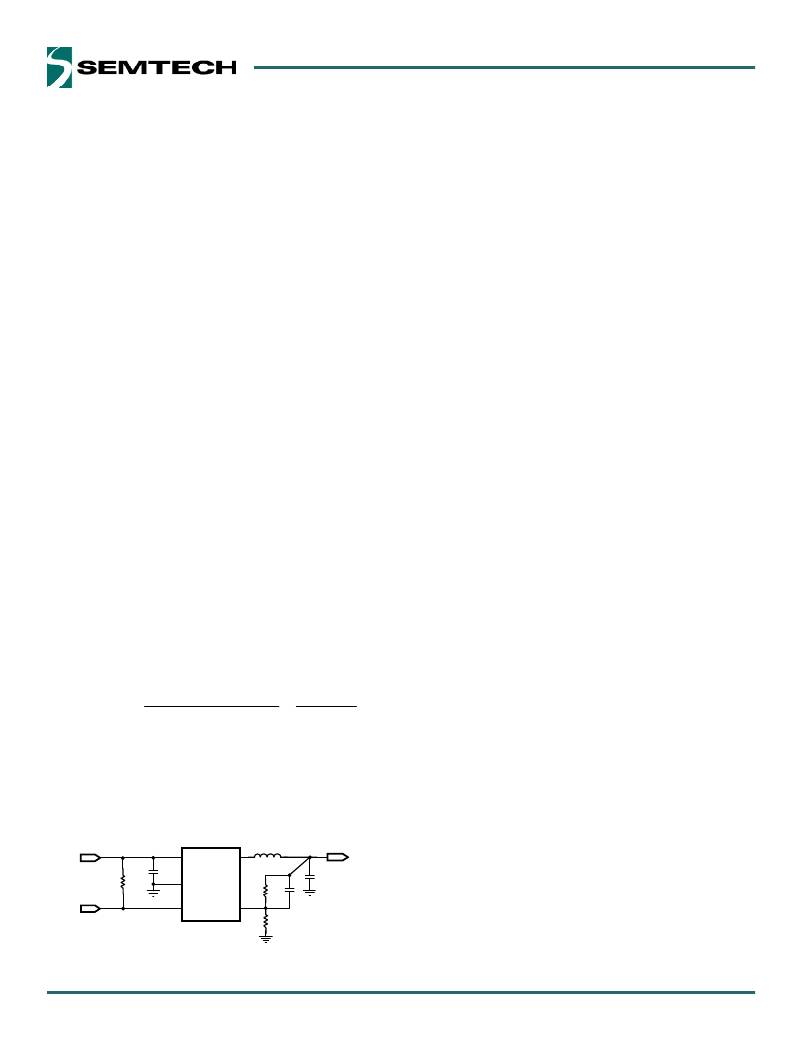
�Figure� 1� with� a� proper� C� FF� calculated� from� the� equation�
�To� simplify� the� design,� it� is� recommended� to� program� the�
�voltage� V� OUT� from� 1.0V as� V� OUT� indesired� of�
�Schematic� output� Adjustable� from� standard� SC189A� (Std� shown� =1.0V)� Current� Limit�
�The� internal� PMOS� power� device� in� the� switching� stage� is�
�protected� by� current� limit� feature.� If� the� output� is� loaded�
�VIN�
�V� LX� V�
�C�
�C�
�R�
�R� C�
�R� FB� 1� =� (� V� OUT� ?� 1� )� � R� FB� 2�
�R�
�10k� ?�
�L�
�IN� OUT�
�IN�
�OUT�
�EN� GND�
�FB1� FF�
�Enable� EN� VOUT�
�FB2�
�SC189A�
�Figure� 1� —� Typical� schematic� for� adjustable� output�
�voltage� option� from� standard� 1.0V� of� SC189A�
�above� the� PMOS� current� limit� for� 32� consecutive� cycles,�
�the� SC189� enters� foldback� current� limit� mode� and� the�
�output� current� is� limited� to� the� current� limit� holding�
�current� (I� CL_HOLD� )� of� a� few� hundred� milliampere.� Under�
�these� conditions� the� output� voltage� will� be� the� product�
�of� I� CL_HOLD� and� the� load� resistance.� The� current� limit�
�holding� current� (I� CL_HOLD� )� will� be� decreased� when� output�
�voltage� is� increased.� The� load� presented� must� fall� below�
�?� 2009� Semtech� =10k� ?� and� C�
�Corp.�
�(2)� R� =10nF� for� standard� design.�
�Note:� (1)� R� EN� is� optional.�
�FB2� FF�
�16�
�www.semtech.com�
�相关PDF资料 |
PDF描述 |
|---|---|
| RMM10DSEI | CONN EDGECARD 20POS .156 EYELET |
| MAX6419UK49+T | IC RESET MPU LOW PWR SOT23-5 |
| RMM12DRXS | CONN EDGECARD 24POS DIP .156 SLD |
| HSC15DREF-S13 | CONN EDGECARD 30POS .100 EXTEND |
| MAX6419UK38+T | IC RESET MPU LOW PWR SOT23-5 |
相关代理商/技术参数 |
参数描述 |
|---|---|
| SC189LULTRT | 功能描述:IC REG BUCK SYNC 1.8V 1.5A 6MLPD RoHS:是 类别:集成电路 (IC) >> PMIC - 稳压器 - DC DC 开关稳压器 系列:- 设计资源:Design Support Tool 标准包装:1 系列:- 类型:升压(升压) 输出类型:固定 输出数:1 输出电压:3V 输入电压:0.75 V ~ 2 V PWM 型:- 频率 - 开关:- 电流 - 输出:100mA 同步整流器:是 工作温度:-40°C ~ 85°C 安装类型:表面贴装 封装/外壳:SOT-23-5 细型,TSOT-23-5 包装:剪切带 (CT) 供应商设备封装:TSOT-23-5 其它名称:AS1323-BTTT-30CT |
| SC189NEVB | 制造商:SEMTECH 制造商全称:Semtech Corporation 功能描述:2.5MHz, 1.5A Synchronous Step Down Regulator |
| SC189NEVB-1 | 制造商:SEMTECH 制造商全称:Semtech Corporation 功能描述:2.5MHz, 1.5A Synchronous Step Down Regulator |
| SC189NULTRT | 制造商:SEMTECH 制造商全称:Semtech Corporation 功能描述:2.5MHz, 1.5A Synchronous Step Down Regulator |
| SC189TEVB | 制造商:SEMTECH 制造商全称:Semtech Corporation 功能描述:2.5MHz, 1.5A Synchronous Step Down Regulator |
发布紧急采购,3分钟左右您将得到回复。