- 您现在的位置:买卖IC网 > PDF目录14783 > SC189LSKTRT (Semtech)IC REG BUCK SYNC 1.8V SOT23-5 PDF资料下载
参数资料
| 型号: | SC189LSKTRT |
| 厂商: | Semtech |
| 文件页数: | 19/24页 |
| 文件大小: | 0K |
| 描述: | IC REG BUCK SYNC 1.8V SOT23-5 |
| 标准包装: | 1 |
| 类型: | 降压(降压) |
| 输出类型: | 固定 |
| 输出数: | 1 |
| 输出电压: | 1.8V |
| 输入电压: | 2.9 V ~ 5.5 V |
| PWM 型: | 电压模式 |
| 频率 - 开关: | 2.5MHz |
| 电流 - 输出: | 1.5A |
| 同步整流器: | 是 |
| 工作温度: | -40°C ~ 85°C |
| 安装类型: | 表面贴装 |
| 封装/外壳: | SC-74A,SOT-753 |
| 包装: | 标准包装 |
| 供应商设备封装: | SOT-23-5 |
| 产品目录页面: | 1357 (CN2011-ZH PDF) |
| 其它名称: | SC189LSKDKR |
�� �
�
�SC189�
�Applications� Information� (continued)�
�compensation� is� designed� to� work� with� a� output� filter�
�corner� frequency� of� less� than� 100kHz� over� any� operating�
�condition,� tolerance� and� bias� effect.� The� corner� frequency�
�of� output� filter� can� be� defined� by� the� equation�
�minimum� gap� possible� to� limit� the� distance� that� magnetic�
�fields� can� radiate� from� the� inductor.� However� shielded�
�inductors� typically� have� a� higher� DCR� and� are� thus� less�
�efficient� than� a� similar� sized� non-shielded� inductor.�
�f� C�
�2�
�1�
�L� C� OUT�
�The� SC189� is� compatible� with� small� shielded� chip� inductors�
�for� low� cost,� low� profile� applications.� The� inductance� roll�
�off� characteristic� of� chip� inductor� is� worse� resulting� in�
�high� ripple� current� and� increased� output� voltage� ripple�
�Values� outside� this� range� may� lead� to� instability,�
�malfunction,� or� out-of-specification� performance.�
�When� choosing� an� inductor,� it� is� important� to� consider�
�the� change� in� inductance� with� DC� bias� current.� The�
�inductor� saturation� current� is� specified� as� the� current� at�
�which� the� inductance� drops� a� specific� percentage� from�
�the� nominal� value.� This� is� approximately� 30%.� Except� for�
�short-circuit� or� other� fault� conditions,� the� peak� current�
�must� always� be� less� than� the� saturation� current� specified�
�by� the� manufacturer.� The� peak� current� is� the� maximum�
�load� current� plus� one� half� of� the� inductor� ripple� current� at�
�at� heavy� load� operation.� SC189� has� OCP� peak� inductor�
�current� threshold� of� 2.0A� minimum,� to� support� 1.5A� DC�
�load� current,� the� inductor� ripple� current� at� 1.5A� DC� load�
�current� needs� to� be� less� than� 1A.�
�Final� inductor� selection� depends� on� various� design�
�considerations� such� as� efficiency,� EMI,� size,� and� cost.� Table�
�2a� and� 2b� list� the� manufacturers� of� recommended� inductor�
�and� output� capacitors.� Chip� inductors� provide� smaller�
�footprint� and� height� with� lower� efficiency� and� increased�
�output� voltage� ripple.� Transient� load� performance� is�
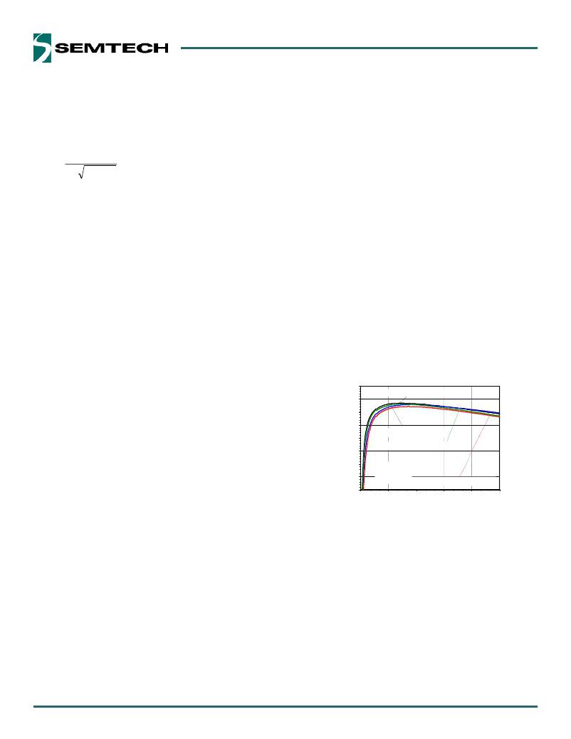
�equivalent� to� wire� wound� inductors.� Figure� 6� shows� the�
�V� IN� =� 5.0V�
�the maximum input voltage. Load and/or line transients�
�can� cause� the� peak� current� to� exceed� his� level� for� short�
�durations.� Maintaining� the� peak� current� below� the�
�inductor� saturation� specification� keeps� the� inductor� ripple�
�current� and� the� output� voltage� ripple� at� acceptable� levels.�
�Manufacturers� often� provide� graphs� of� actual� inductance�
�and� saturation� characteristics� versus� applied� inductor�
�current.� The� saturation� characteristics� of� the� inductor� can�
�vary� significantly� with� core� temperature.� Core� and� ambient�
�temperatures� should� be� considered� when� examining� the�
�core� saturation� characteristics.�
�typical� efficiency� curves� for� different� inductors.�
�Efficiency�
�100%�
�L=1071AS-2R2N� (50m� ?� _typ)�
�95%�
�90%�
�85%�
�L=1071AS-1R0N� (33m� ?� _typ)�
�80%�
�L=MDT2520-CR1R0M� (60m� ?� _typ)�
�75%�
�70%�
�V� OUT� =� 3.3V�
�65%�
�T� A� =25°C� L=LQM2HP1R0MG0� (55m� ?� _typ)�
�60%�
�0.0� 0.3� 0.6� 0.9� 1.2�
�Output� Current� (A)�
�1.5�
�When� the� inductance� has� been� determined,� the� DC�
�resistance� (DCR)� must� be� examined.� The� efficiency� that�
�can� be� achieved� is� dependent� on� the� DCR� of� the� inductor.�
�The� lower� values� give� higher� efficiency.� The� RMS� DC�
�current� rating� of� the� inductor� is� associated� with� losses� in�
�the� copper� windings� and� the� resulting� temperature� rise� of�
�the� inductor.� This� is� usually� specified� as� the� current� which�
�produces� a� 40?C� temperature� rise.� Most� copper� windings�
�are� rated� to� accommodate� this� temperature� rise� above�
�maximum� ambient.�
�Magnetic� fields� associated� with� the� output� inductor� can�
�interfere� with� nearby� circuitry.� This� can� be� minimized� by�
�the� use� of� low� noise� shielded� inductors� which� use� the�
�Figure� 6� —� Typical� efficiency� curves�
�(V� IN� =5.0V,� V� OUT� =3.3V)�
�C� OUT� Selection�
�The� internal� voltage� loop� compensation� in� the� SC189� limits�
�the� minimum� output� capacitor� value� to� 10μF� if� using� the�
�inductor� of� 2.2μH.� This� is� due� to� its� influence� on� the� the�
�loop� crossover� frequency,� phase� margin,� and� gain� margin.�
�Increasing� the� output� capacitor� above� this� minimum�
�value� will� reduce� the� crossover� frequency� and� provide�
�greater� phase� margin.� A� total� output� capacintance� should�
�not� exceed� 30uF� to� avoid� any� start-up� problems.� For� most�
�typical� applications,� it� is� recommended� to� use� output�
�capacitance� of� 10uF� to� 22uF.� When� choosing� output�
�?� 2009� Semtech� Corp.�
�19�
�www.semtech.com�
�相关PDF资料 |
PDF描述 |
|---|---|
| RMM10DSEI | CONN EDGECARD 20POS .156 EYELET |
| MAX6419UK49+T | IC RESET MPU LOW PWR SOT23-5 |
| RMM12DRXS | CONN EDGECARD 24POS DIP .156 SLD |
| HSC15DREF-S13 | CONN EDGECARD 30POS .100 EXTEND |
| MAX6419UK38+T | IC RESET MPU LOW PWR SOT23-5 |
相关代理商/技术参数 |
参数描述 |
|---|---|
| SC189LULTRT | 功能描述:IC REG BUCK SYNC 1.8V 1.5A 6MLPD RoHS:是 类别:集成电路 (IC) >> PMIC - 稳压器 - DC DC 开关稳压器 系列:- 设计资源:Design Support Tool 标准包装:1 系列:- 类型:升压(升压) 输出类型:固定 输出数:1 输出电压:3V 输入电压:0.75 V ~ 2 V PWM 型:- 频率 - 开关:- 电流 - 输出:100mA 同步整流器:是 工作温度:-40°C ~ 85°C 安装类型:表面贴装 封装/外壳:SOT-23-5 细型,TSOT-23-5 包装:剪切带 (CT) 供应商设备封装:TSOT-23-5 其它名称:AS1323-BTTT-30CT |
| SC189NEVB | 制造商:SEMTECH 制造商全称:Semtech Corporation 功能描述:2.5MHz, 1.5A Synchronous Step Down Regulator |
| SC189NEVB-1 | 制造商:SEMTECH 制造商全称:Semtech Corporation 功能描述:2.5MHz, 1.5A Synchronous Step Down Regulator |
| SC189NULTRT | 制造商:SEMTECH 制造商全称:Semtech Corporation 功能描述:2.5MHz, 1.5A Synchronous Step Down Regulator |
| SC189TEVB | 制造商:SEMTECH 制造商全称:Semtech Corporation 功能描述:2.5MHz, 1.5A Synchronous Step Down Regulator |
发布紧急采购,3分钟左右您将得到回复。