- 您现在的位置:买卖IC网 > PDF目录14782 > SC189ZULTRT (Semtech)IC REG BUCK SYNC 3.3V 1.5A 6MLPQ PDF资料下载
参数资料
| 型号: | SC189ZULTRT |
| 厂商: | Semtech |
| 文件页数: | 21/24页 |
| 文件大小: | 0K |
| 描述: | IC REG BUCK SYNC 3.3V 1.5A 6MLPQ |
| 标准包装: | 1 |
| 类型: | 降压(降压) |
| 输出类型: | 固定 |
| 输出数: | 1 |
| 输出电压: | 3.3V |
| 输入电压: | 2.9 V ~ 5.5 V |
| PWM 型: | 电压模式 |
| 频率 - 开关: | 2.5MHz |
| 电流 - 输出: | 1.5A |
| 同步整流器: | 是 |
| 工作温度: | -40°C ~ 85°C |
| 安装类型: | 表面贴装 |
| 封装/外壳: | 6-MLPD-UT |
| 包装: | 标准包装 |
| 供应商设备封装: | 6-MLPD-UT(2x2) |
| 产品目录页面: | 1357 (CN2011-ZH PDF) |
| 其它名称: | SC189ZULDKR |
�� �
�
�SC189�
�Applications� Information� (continued)�
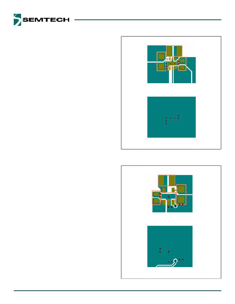
�PCB� Layout� Considerations�
�The� layout� diagram� in� figure� 7� and� figure� 8� shows� a�
�recommended� PCB� for� MLPD-UT6� 2x2� and� SOT23-5�
�package,� respectively.� Fundamental� layout� rules� must�
�be� followed� since� the� layout� is� critical� for� achieving� the�
�performance� specified� in� the� Electrical� Characteristics�
�VOUT�
�L�
�GND�
�table.� Poor� layout� can� degrade� the� performance� of� the� DC-�
�DC� converter� and� can� contribute� to� EMI� problems,� ground�
�bounce,� and� resistive� voltage� losses.� Poor� regulation� and�
�instability� can� result.�
�The� following� guidelines� are� recommended� when�
�developing� a� PCB� layout:�
�1.� The� input� capacitor,� C� IN� should� be� placed� as� close� to� the�
�VIN� and� GND� pins� as� possible.� This� capacitor� provides�
�a� low� impedance� loop� for� the� pulsed� currents� present�
�at� the� buck� converter� ’s� input.� Use� short� wide� traces�
�to� connect� as� closely� to� the� IC� as� possible.� This� will�
�minimize� EMI� and� input� voltage� ripple� by� localizing�
�the� high� frequency� current� pulses.�
�2.� Keep� the� LX� pin� traces� as� short� as� possible� to� minimize�
�pickup� of� high� frequency� switching� edges� to� other�
�parts� of� the� circuit.� C� OUT� and� L� should� be� connected� as�
�close� as� possible� between� the� LX� and� GND� pins,� with�
�a� direct� return� to� the� GND� pin� from� C� OUT� .�
�3.� Route� the� output� voltage� feedback/sense� path� away�
�U1�
�GND�
�VIN�
�EN�
�(a)� Top� layer� for� MLPD-UT6� 2x2� package�
�GND�
�GND�
�(b)� Bottom� layer� for� MLPD� 2x2� package�
�Figure� 7� —� Recommended� PCB� Top� &� Bottom� Layer�
�Layout� for� MLPD-UT6� 2x2� Package�
�from� inductor� and� LX� node� to� minimize� noise� and�
�magnetic� interference.�
�4.� Use� a� ground� plane� referenced� to� the� SC189� GND� pin.�
�Use� several� vias� to� connect� to� the� component� side�
�ground� to� further� reduce� noise� and� interference� on�
�C� IN�
�L�
�VOUT�
�C� OUT�
�sensitive� circuit� nodes.�
�5.� If� possible,� minimize� the� resistance� from� the� VOUT� and�
�VIN�
�U1�
�GND�
�GND� pins� to� the� load.� This� will� reduce� the� voltage� drop�
�on� the� ground� plane� and� improve� the� load� regulation.�
�And� it� will� also� improve� the� overall� efficiency� by�
�reducing� the� copper� losses� on� the� output� and� ground�
�planes.�
�(a)� Top� layer� for� SOT23-5� package�
�GND�
�EN�
�(b)� Bottom� layer� for� SOT23-5� package�
�Figure� 8� —� Recommended� PCB� Top� &� Bottom� Layer�
�Layout� for� SOT23-5� Package�
�?� 2009� Semtech� Corp.�
�21�
�www.semtech.com�
�相关PDF资料 |
PDF描述 |
|---|---|
| LGU1E153MELA | CAP ALUM 15000UF 25V 20% SNAP |
| MAX6426UK20+T | IC MPU/RESET CIRC 2.00V SOT23-5 |
| ECC30DRTI-S734 | CONN EDGECARD 60POS DIP .100 SLD |
| ECA22DRST-S288 | CONN EDGECARD 44POS .125 EXTEND |
| V72C28T150B2 | CONVERTER MOD DC/DC 28V 150W |
相关代理商/技术参数 |
参数描述 |
|---|---|
| SC18IM700 | 制造商:PHILIPS 制造商全称:NXP Semiconductors 功能描述:Master I2C-bus controller with UART interface |
| SC18IM700IPW | 制造商:PHILIPS 制造商全称:NXP Semiconductors 功能描述:Master I-2C - bus controller with UART interface |
| SC18IM700IPW,112 | 功能描述:UART 接口集成电路 CTRL I2C W/UART RoHS:否 制造商:Texas Instruments 通道数量:2 数据速率:3 Mbps 电源电压-最大:3.6 V 电源电压-最小:2.7 V 电源电流:20 mA 最大工作温度:+ 85 C 最小工作温度:- 40 C 封装 / 箱体:LQFP-48 封装:Reel |
| SC18IM700IPW,128 | 功能描述:UART 接口集成电路 UART-MASTER I2C RoHS:否 制造商:Texas Instruments 通道数量:2 数据速率:3 Mbps 电源电压-最大:3.6 V 电源电压-最小:2.7 V 电源电流:20 mA 最大工作温度:+ 85 C 最小工作温度:- 40 C 封装 / 箱体:LQFP-48 封装:Reel |
| SC18IM700IPW/S8HP | 功能描述:IC CTRL I2CW/UART 16TSSOP 制造商:nxp usa inc. 系列:- 零件状态:在售 协议:I2C 功能:控制器 接口:UART 标准:- 电压 - 电源:2.4 V ~ 3.6 V 电流 - 电源:9mA 工作温度:-40°C ~ 85°C 封装/外壳:16-TSSOP(0.173",4.40mm 宽) 供应商器件封装:16-TSSOP 标准包装:1 |
发布紧急采购,3分钟左右您将得到回复。